Led with scattering features in substrate

A substrate and light scattering technology, applied in semiconductor devices, electrical components, circuits, etc., can solve problems such as reducing the light extraction efficiency of LED dies

Active Publication Date: 2016-04-27
LUMILEDS HLDG BV
View PDF7 Cites 15 Cited by
  • Summary
  • Abstract
  • Description
  • Claims
  • Application Information

AI Technical Summary

Problems solved by technology

[0006] All absorbing regions reduce the light extraction efficiency of the LED die

Method used


Image

  • Led with scattering features in substrate
  • Led with scattering features in substrate
  • Led with scattering features in substrate

Examples


Embodiment Construction

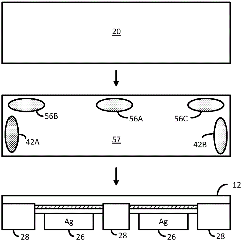
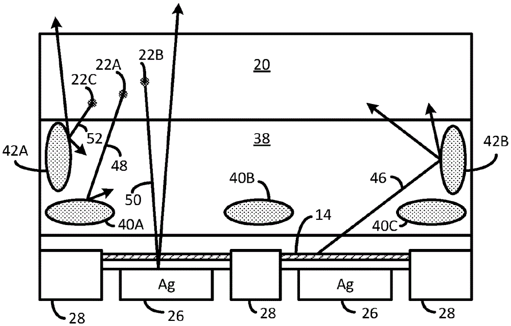
[0023] figure 2 Illustrates that in addition to the substrate 38 can be used with figure 1 The LED die 10 in the same LED36. Substrate 38 may be a growth substrate on which the LED semiconductor has been epitaxially grown, or may be a substrate that has been attached to the LED semiconductor layer after the growth substrate has been removed.

[0024] Substrate 38 is formed with light scattering regions 40A, 40B, and 40C over some or all of the light absorbing regions and with light scattering regions 42A and 42B over some or all of the sidewalls to reduce light guidance within substrate 38 . Scattering regions 42A and 42B may be part of a continuous ring of scattering regions around the sidewalls.

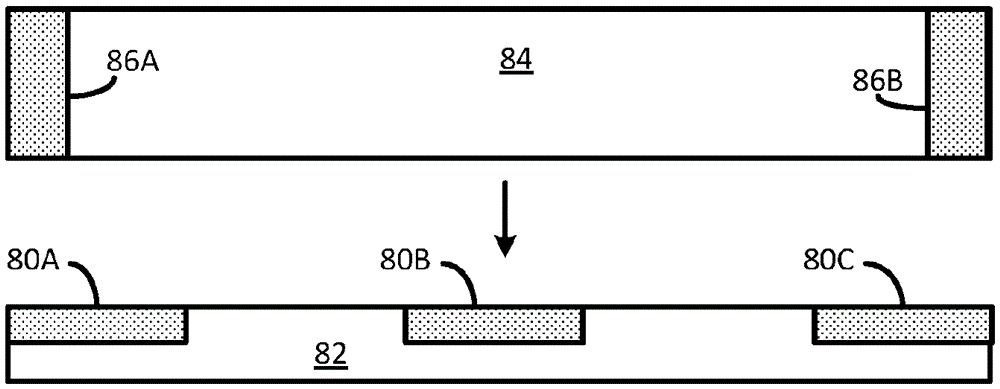
[0025] In one embodiment, substrate 38 is a sapphire growth substrate on which LED semiconductor layers have been epitaxially grown. Scattering regions 40A- 40C, 42A and 42B may be formed as an array of voids before or after growing the semiconductor layer. Scattering regions ...


PUM


Abstract

In one embodiment, the transparent growth substrate (38) of an LED die is formed to have light scattering areas (40A-C), such as voids formed by a laser. In another embodiment, the growth substrate is removed and replaced by another substrate that is formed with light scattering areas. In one embodiment, the light scattering areas are formed over the light absorbing areas of the LED die, to reduce the amount of incident light on those absorbing areas, and over the sides (42A, 42B) of the substrate to reduce light guiding. Another embodiment comprises a replacement substrate may be formed to include reflective particles in selected areas where there are no corresponding light generating areas in the LED semiconductor layers such as -type metal contacts (28). This prevents reabsorption into absorbing regions of the semiconductor layer thereby enhancing external efficiency of the device. A 3D structure may be formed by stacking substrate layers containing the reflective areas. The substrate may be a transparent substrate or a phosphor tile (20) that is affixed to the top of the LED.

Description

technical field [0001] The present invention relates to light emitting diodes (LEDs), and in particular to techniques for scattering light within an LED die. Background technique [0002] In GaN-based LEDs that emit blue light, the growth substrate is typically a transparent sapphire substrate, a SiC substrate or even a GaN substrate. With flip-chip LEDs, light is generated by the active layer and exits through the transparent substrate. [0003] figure 1 A conventional GaN-based flip-chip LED die 10 is illustrated. The semiconductor layer includes an N-type layer 12 , an active layer 14 (forming a quantum well) and a P-type layer 16 . These layers are grown on the surface of a transparent growth substrate 18, typically sapphire. A phosphor layer 20 is deposited on top of the substrate 18 . The phosphor particles 22 are excited by the blue light emitted by the active layer 14 and shift the wavelength of the light. If the color emitted by the phosphor is yellow, the com...

Claims


Application Information

Patent Timeline
Patent Type & Authority Applications(China)
IPC IPC(8): H01L33/02H01L33/50
CPCH01L33/02H01L33/501H01L33/508H01L2933/0091H01L33/502H01L33/60H01L33/36H01L33/507
Inventor K.范波拉H-H.贝奇特尔
Owner LUMILEDS HLDG BV
Why Eureka
Try Eureka