Holographic waveguide display device
A display device and a holographic waveguide technology, applied in the field of wearable displays, can solve problems such as blurred images, achieve the effects of reducing light energy loss, suppressing stray light, and improving light energy utilization
- Summary
- Abstract
- Description
- Claims
- Application Information
AI Technical Summary
Problems solved by technology
Method used
Image

Examples
Embodiment Construction
[0016] The technical scheme of the present invention is described in detail below in conjunction with accompanying drawing:
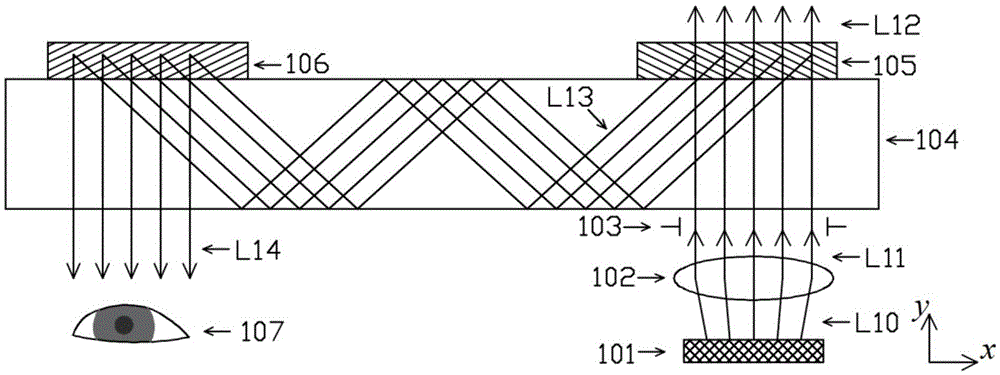
[0017] The structural principle of a holographic waveguide display device in the prior art is as follows: figure 1 As shown, it includes a microdisplay 101 , a collimating mirror 102 , an aperture 103 , a waveguide 104 , an in-coupling holographic optical element 105 , and an out-coupling holographic optical element 106 . Such as figure 1 As shown, in the working process of the display device, the microdisplay 101 emits divergent light L10 with image information outward, and the divergent light L10 passes through the collimating mirror 102 and is converted into parallel light L11, and the parallel light L11 is captured by the diaphragm 103 Limiting the size of the aperture, it is incident vertically on the surface of the in-coupling holographic optical element 105, and a part of the TM polarization component passes through 105 to be the transmitted lig...
PUM
| Property | Measurement | Unit |
|---|---|---|
| Thickness | aaaaa | aaaaa |
| Thickness | aaaaa | aaaaa |
Abstract
Description
Claims
Application Information