

Shift register and drive method thereof
A shift register, low-potential technology, applied in static memory, digital memory information, instruments, etc., can solve the problems that cannot be applied to various driving methods of flat-panel display devices, and that shift registers cannot realize various types and methods of shifting. Bit and other issues, to achieve the effect of low-level trigger type signal shift and overall shift
- Summary
- Abstract
- Description
- Claims
- Application Information
AI Technical Summary
Problems solved by technology
Method used
Image

Examples
Embodiment 1
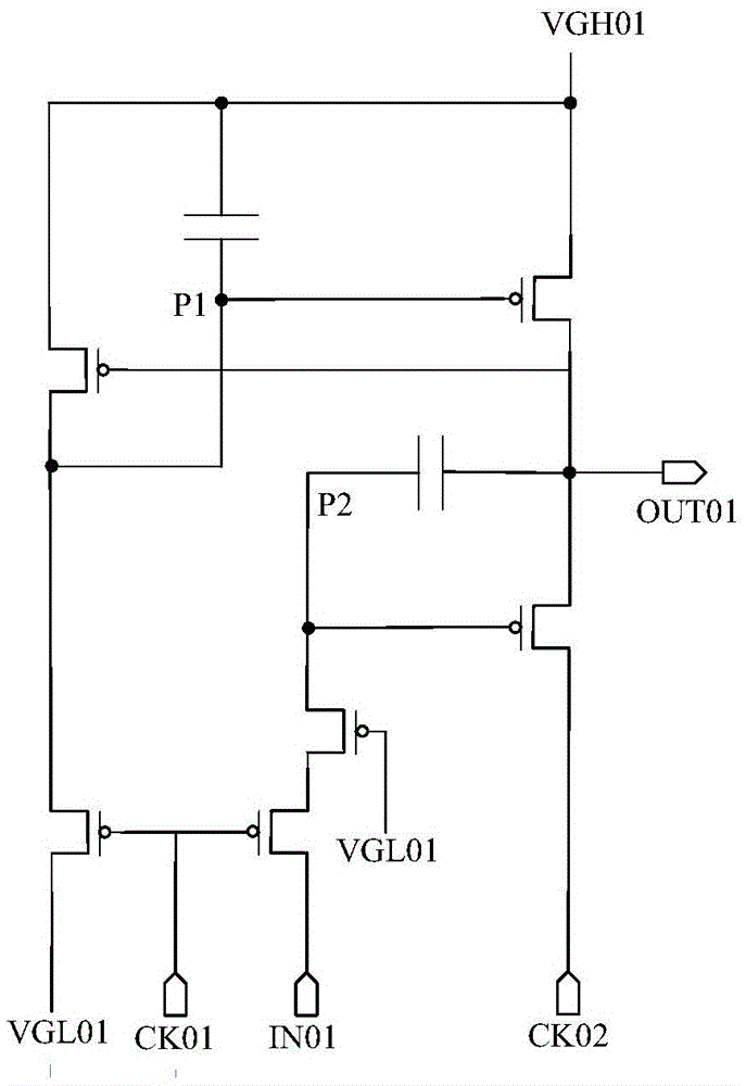
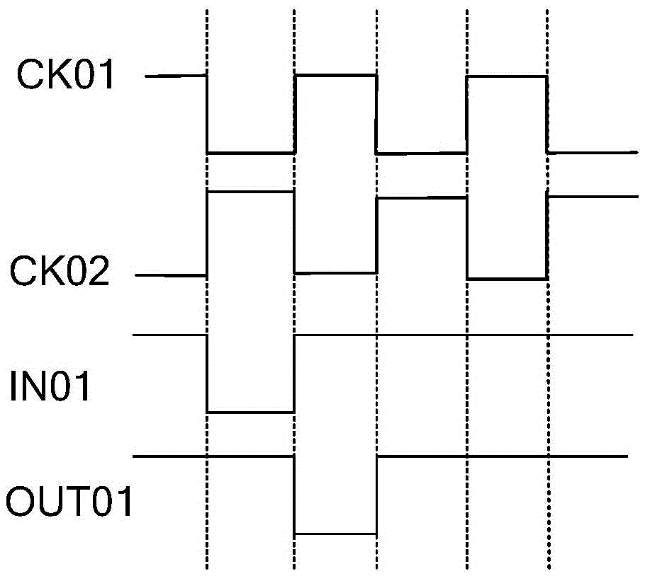
[0038] Embodiment 1 of the present invention provides a shift register, such as image 3 Shown is the specific circuit structure of the shift register.
[0039]In Embodiment 1 of the present invention, the shift register includes: a first module 11, configured to generate a first voltage signal according to a first reference voltage and a second reference voltage in response to an input signal and a first control signal, and the input signal is When the potential is high, the first voltage signal becomes low potential under the trigger of the first control signal. The second module 12 is configured to generate a second voltage signal according to the input signal and the first reference voltage signal in response to the first voltage signal and the second control signal; when the input signal is at a low potential, the The second voltage signal becomes a low potential under the trigger of the second control signal; the third module 13 is configured to generate a third voltage...
Embodiment 2
[0078] Embodiment 2 of the present invention provides a shift register on the basis of Embodiment 1, such as Figure 5 Shown is the specific circuit structure of the shift register.
[0079] The difference from Embodiment 1 is that the first module 21 of the shift register is also used to respond to a third control signal, and when the input signal is at a low potential, the first voltage signal is controlled by the third control signal. When the signal is triggered, it becomes a high potential; the third control signal is a clock signal with the same frequency as the first control signal.
[0080] Specifically, the third control signal is the second clock signal CK.
[0081] Wherein, on the basis of the circuit structure of the first embodiment, the first module 21 further includes a fourth switching transistor T4 coupled between the second switching transistor T2 and the second node N2, and the fourth switching transistor T4 The third control signal CK is input to the gate...
Embodiment 3
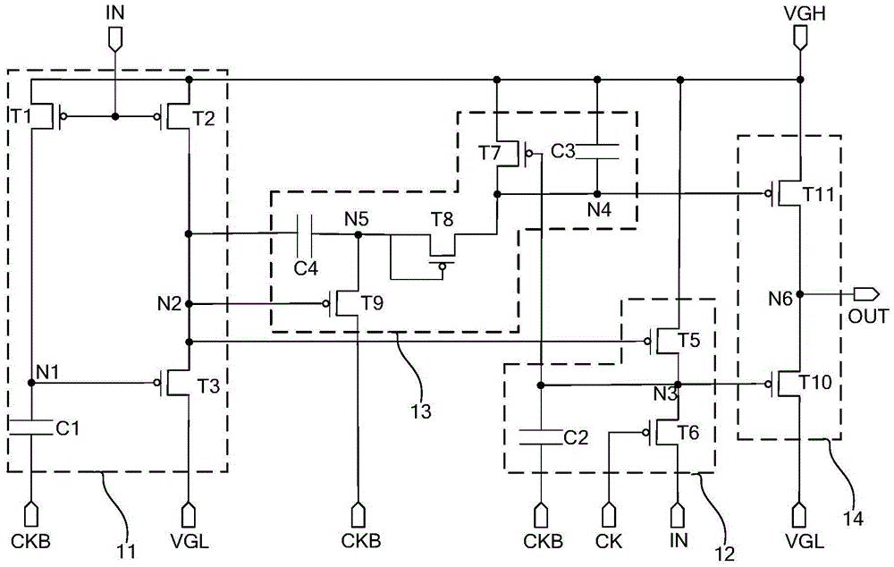
[0106] Embodiment 3 of the present invention provides a shift register on the basis of Embodiment 2, such as Figure 8 Shown is the specific circuit structure of the shift register.
[0107] The difference from the second embodiment is that the first control signal of the first module 31 of the shift register is the second clock signal CK, and the fourth control signal of the third module 33 of the shift register is the second clock signal CK, and, in the third module 33, the second electrode of the ninth switching transistor is electrically connected to the second reference voltage VGL.
[0108] Below, according to Figure 9 The sequence diagram in Figure 8 The working process of the shift register shown in different stages is further described.
[0109] specific, Figure 9 The input signal IN in is a high-level trigger type signal, and the shift register implements a 1:1 overlap shift.
[0110] At time T1, the input signal IN is at a low potential, the first switching ...
PUM
 Abstract
Description
Claims
Application Information