A connection device between jtag interface and internal user logic

A technology for internal users and connecting devices, applied in the field of JTAG, can solve the problems of low timing performance of logic resource system, too many interface connections, occupying FPGA wiring resources, etc., to improve timing performance, reduce wiring resources, and simplify processing Effect

Active Publication Date: 2018-05-04
SHENZHEN PANGO MICROSYST CO LTD
View PDF3 Cites 0 Cited by
  • Summary
  • Abstract
  • Description
  • Claims
  • Application Information

AI Technical Summary

Problems solved by technology

[0004] In the process of realizing the present invention, the inventor finds that there are at least the following technical problems in the prior art: the controller processing module has too many interface connections to the internal user logic, which will take up too many FPGA wiring resources. As a core processing module, it takes up more logic resources, which makes the timing performance of the system not high.

Method used


Image

  • A connection device between jtag interface and internal user logic
  • A connection device between jtag interface and internal user logic
  • A connection device between jtag interface and internal user logic

Examples


Embodiment Construction

[0021] In order to make the purpose, technical solutions and advantages of the embodiments of the present invention clearer, the technical solutions in the embodiments of the present invention will be clearly and completely described below in conjunction with the drawings in the embodiments of the present invention. Obviously, the described embodiments It is only some embodiments of the present invention, but not all embodiments. Based on the embodiments of the present invention, all other embodiments obtained by persons of ordinary skill in the art without making creative efforts belong to the protection scope of the present invention.

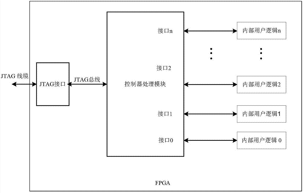
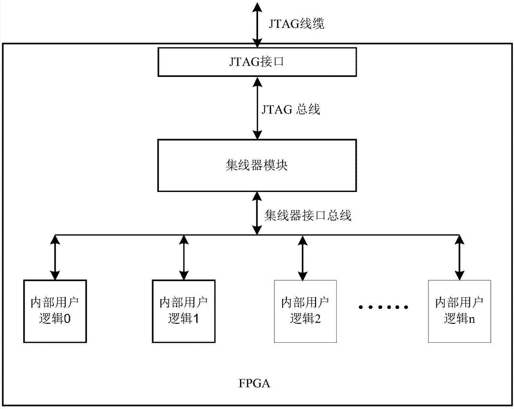
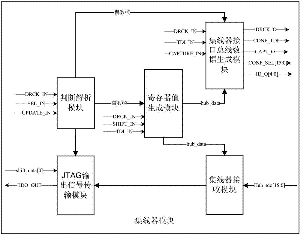
[0022] In JTAG debugging, Boundary-Scan is a very important concept. The basic idea of ​​boundary scan technology is to add a shift register unit on the input and output pins close to the chip. Because these shift register units are distributed on the boundary (surrounding) of the chip, they are called boundary-scan registers (Boundary-ScanR...


PUM


Abstract

The invention provides a JTAG interface and internal user logic connecting device. The JTAG interface and internal user logic connecting device comprises a concentrator module, a JTAG interface is connected with the concentrator module through a JTAG bus, the concentrator module is connected with multiple internal user logics through a concentrator interface bus, and the multiple internal user logics select communication through chip select signals corresponding to the internal user logics. The JTAG interface and internal user logic connecting device is only provided with one bus, wiring resources of chips are decreased, and the timing sequence performance is improved.

Description

technical field [0001] The invention relates to the technical field of JTAG, in particular to a connection device between a JTAG interface and user logic inside a chip. Background technique [0002] In recent years, with the development of microprocessor technology, more and more processors and logic devices use the JTAG (Joint Test Action Group) interface as an intermediary between their cores and PCs. The JTAG interface is a boundary-scan protocol specified in IEEE1149.1. The JTAG protocol is often used for internal testing of chips. Most advanced devices now support the JTAG protocol, such as ARM, DSP, and FPGA (Field-Programmable Gate Array) devices. In the FPGA, the JTAG interface can be used as a part of the configuration function module. The PC can program and configure the FPGA through the JTAG interface, and can also access the internal user logic (User APP IP) through the JTAG interface. User APP IP can be debugging tools, such as embedded Debugcore logic analyzer...

Claims


Application Information

Patent Timeline
Patent Type & Authority Patents(China)
IPC IPC(8): G06F13/40G06F13/42G06F13/38
CPCG06F13/38G06F13/4068G06F13/42
Inventor 李宁
Owner SHENZHEN PANGO MICROSYST CO LTD
Why Eureka
Try Eureka