A test substrate and a probe card manufactured using the test substrate

A technology for testing substrates and test terminals, which is applied in the field of probe cards, and can solve the problems of small TSVs, inability to detect TSVs, and inapplicable wafer detection for 3D chips.

Active Publication Date: 2016-07-06
SHANDONG INST OF ADVANCED TECH CHINESE ACAD OF SCI CO LTD
View PDF7 Cites 0 Cited by
  • Summary
  • Abstract
  • Description
  • Claims
  • Application Information

AI Technical Summary

Problems solved by technology

[0010] The technical problem to be solved by the present invention is that the size of the chip testing device in the prior art is too large, and the size of the TSVs on the wafer constituting the three-dimensional chip is small and the arrangement density is high, so it is impossible to detect the TSVs one by one at the same time. It is suitable for the detection of three-dimensional chip wafers before packaging, thereby providing a test substrate that can detect each through-silicon hole at the same time, suitable for the detection of three-dimensional chips before chip packaging, and the test substrate manufactured using the test substrate. probe card

Method used


Image

  • A test substrate and a probe card manufactured using the test substrate
  • A test substrate and a probe card manufactured using the test substrate
  • A test substrate and a probe card manufactured using the test substrate

Examples


Embodiment 1

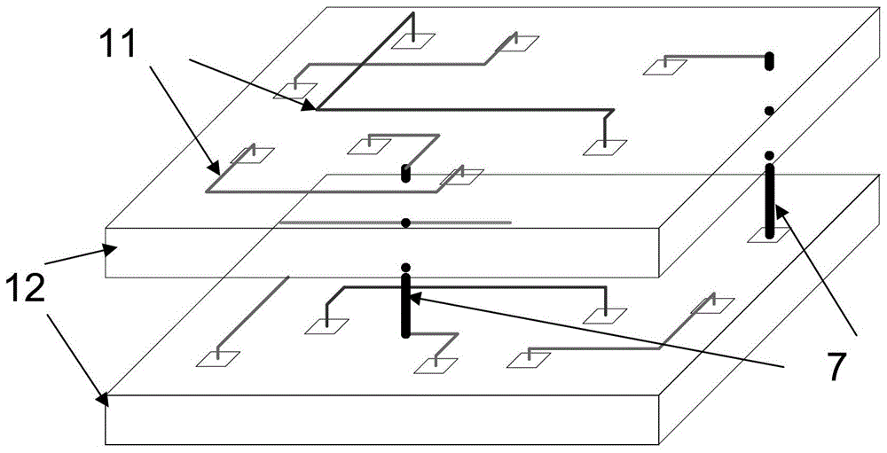
[0050] The test substrate of the present invention is used to test the wafer 10 before stacking, such as Figure 5 , Image 6 shown, including:

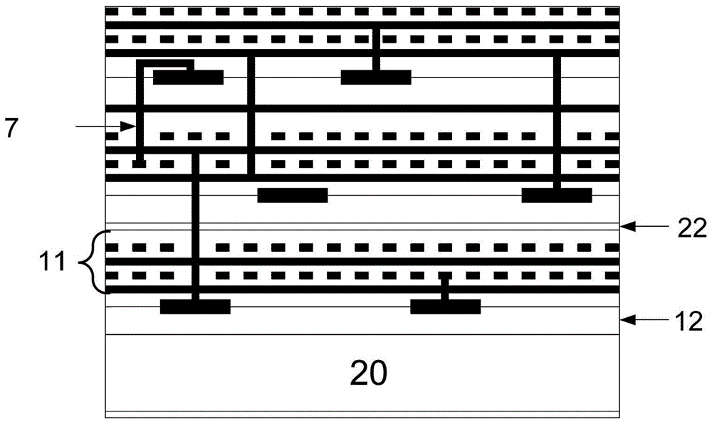
[0051] A plurality of test terminal micro-protrusions 2 are arranged on the top surface of the base 1 of the test substrate according to the same layout as the contact 7 to be tested at the bottom of the wafer 10, and each of the test terminal micro-protrusions 2 It matches the size of the contact 7 to be tested.

[0052] For the three-dimensional chip, the contact 7 to be tested is a through-silicon hole, and the manufacturing process of the through-silicon hole is an existing technology, so it will not be repeated here; The top surface of the base 1 of the test substrate, currently, the etching technology has reached the 20 nanometer level, therefore, the micro-protrusion 2 of the test end can be made small enough, such as 5-10 microns, so the micro-protrusion 2 of the test end The size of the through-silicon via can be made to ...

Embodiment 2

[0068] Because the chip 10 in the 2.5-dimensional chip has no TSV, the following changes can be made on the basis of Embodiment 1:

[0069] In order to perform a pre-stacking test on the wafer 10 constituting a 2.5-dimensional chip, as an optional implementation, micro-protrusions at the end to be tested may be formed on the bottom of the wafer 10 by etching technology as input and output ports for test signals. At present, the etching technology has reached the level of 20 nanometers. Therefore, the micro-protrusion at the terminal to be tested can be made small enough, such as 5-10 microns, to establish signal connection with each device on the wafer 10 through the wafer wiring layer 11 .

[0070] Because the test terminal micro-protrusions 2 on the top surface of the base 1 of the test substrate are arranged according to the same layout of the contact points 7 to be tested at the bottom of the wafer 10, that is, the micro-protrusions of the terminal to be tested, A one-to-o...

Embodiment approach

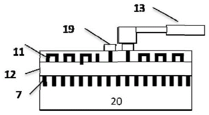
[0072] The test substrates described in Embodiment 1 and Embodiment 2 can also be used to manufacture probe cards, without additional use of test probes 13 to indirectly transmit test signals to the contacts 7 to be tested on the wafer 10 . The implementation is as follows:

[0073] For a test substrate that does not contain contact pads 5, it is only necessary to remove the detection bumps 4 located on the bottom surface of the base 1 of the test substrate, and add wiring to the bottom of the base 1 of the test substrate, and pass the new Adding wiring directly transmits the test signal from the automatic testing machine to each test terminal micro-protrusion 2 on the top surface of the base 1 of the test substrate, and passes through the test terminal micro-protrusion 2 to the test signal located on the test substrate. Each contact 7 to be tested on the bottom of the wafer 10, and the tested signal is output to an automatic testing machine through newly added wiring, so that...


PUM


Abstract

Provided are a test substrate and a probe card manufactured using the test substrate. Test-end micro bulges (2) on a top surface of the test substrate are arranged according to the layout of contacts (7) to be detected at the bottom of a wafer (10) to be detected, are correspondingly connected to through-substrate via holes (3) via top wirings (8) and are electrically conducted, the through-substrate via holes (3) are correspondingly connected to detection bulges (4) on the bottom surface of the test substrate and are electrically conducted, and the detection bulges (4) match test probes (13) in size, so that a one-to-one correspondence signal relationship between the test probes (13) and the test-end micro bulges (2) and the contacts (7) to be detected is established, and the problem that there is no way for the test probes (13) to directly detect each contact (7) to be detected due to the test probes (13) being too big and the contacts (7) to be detected being too small in the related art is solved. By overlaying an anisotropic conductive resin on the top surface of the test substrate, the test-end micro bulges (2) can be electrically conducted without the need for them to come into contact with the contacts (7) to be detected, thereby avoiding damage to the wafer (10) and improving the signal transmission property.

Description

technical field [0001] The invention relates to a test substrate and a probe card manufactured by using the test substrate, in particular to a test substrate used to detect chips in the semiconductor manufacturing industry and a probe card manufactured by using the test substrate, belonging to Electronic testing technology field. Background technique [0002] With the continuous improvement of the chip manufacturing process, the volume of the chip is continuously reduced while the operation speed is continuously improved. However, as the semiconductor manufacturing process enters the deep nanoscale, the performance of the chip can no longer continue to improve as before, mainly due to the following factors: (1) The delay on the chip interconnection has replaced the delay of the device itself, and has become an important factor for increasing the chip rate. (2) With the continuous improvement of integration, more and more devices of different processes are integrated in the ...

Claims


Application Information

Patent Timeline
Patent Type & Authority Patents(China)
IPC IPC(8): G01R1/02G01R1/073
CPCG01R1/07378
Inventor 蒋力徐强李慧云徐国卿苏少博张晓龙
Owner SHANDONG INST OF ADVANCED TECH CHINESE ACAD OF SCI CO LTD
Why Eureka
Try Eureka