Fin type field effect transistor (FET) and formation method thereof

A fin-type field effect and transistor technology, which is applied in semiconductor devices, semiconductor/solid-state device manufacturing, electrical components, etc., can solve problems that cannot meet the needs of device performance, and achieve the effect of improving carrier mobility and performance

Active Publication Date: 2016-05-11
SEMICON MFG INT (SHANGHAI) CORP
View PDF2 Cites 7 Cited by
  • Summary
  • Abstract
  • Description
  • Claims
  • Application Information

AI Technical Summary

Problems solved by technology

However, when the feature size of the device is further reduced, even if the gate-last process is adopted, the structure of the conventional MOS field effect transisto

Method used


Image

  • Fin type field effect transistor (FET) and formation method thereof
  • Fin type field effect transistor (FET) and formation method thereof
  • Fin type field effect transistor (FET) and formation method thereof

Examples


Embodiment Construction

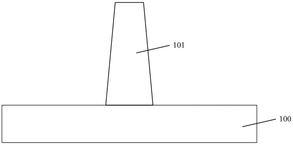
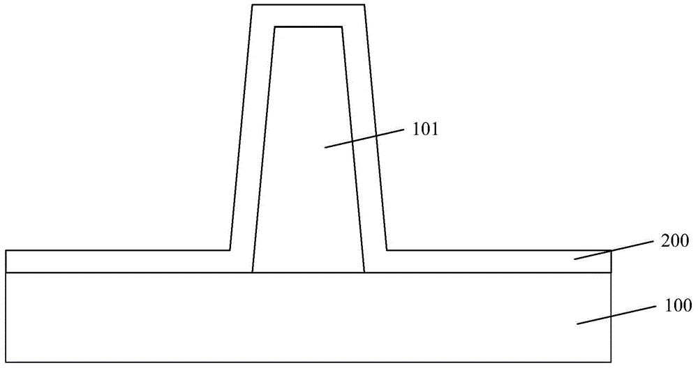
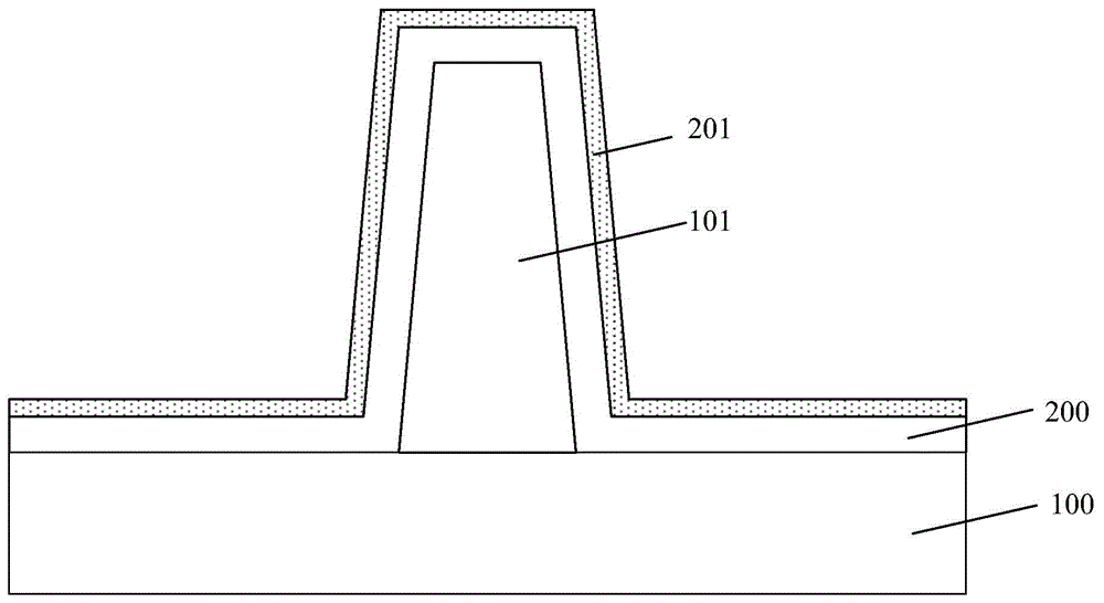
[0031] As mentioned in the background art, the performance of existing fin field effect transistors formed by using graphene as a channel material needs to be further improved.

[0032] The quality of the graphene layer currently formed on the fin is poor, the atomic disorder on the surface of the graphene layer is high, and there are many defects in the graphene layer, resulting in the mobility of the charge carriers in the graphene layer. Decrease, thereby affecting the performance of the formed fin field effect transistor.

[0033] In the embodiment of the present invention, a graphene layer is formed with a carbon-containing semiconductor layer as a base, and the graphene layer is subjected to surface treatment to eliminate defects of the graphene layer, and then a gate is formed on the surface of the graphene layer. The pole structure can improve the quality of the graphene layer and improve the performance of the formed fin field effect transistor.

[0034] In order to ...


PUM


Abstract

The invention relates to a fin type FET and a formation method thereof. The formation method comprises that a semiconductor substrate is provided; a fin portion is formed on the semiconductor substrate; a carbon-contained semiconductor layer is formed at the surface of the fin portion and the semiconductor substrate; a graphene layer is formed at the surface of the carbon-contained semiconductor layer; the surface of the graphene layer is restored to eliminate defects of the graphene layer; an isolation layer is formed on part of the graphene layer, and the surface of the isolation layer is lower than the top surface of the fin portion; and a grid structure across the fin portion is formed at the surface of the graphene layer, and the grid structure covers the part, placed at the top and the sidewalls of the fin portion, of the graphene layer. The method can improve the performance of the fin type FET.

Description

technical field [0001] The invention relates to the technical field of semiconductors, in particular to a fin field effect transistor and a forming method thereof. Background technique [0002] With the continuous development of semiconductor process technology, process nodes are gradually reduced, and gate-last (gate-last) process has been widely used to obtain an ideal threshold voltage and improve device performance. However, when the feature size of the device is further reduced, even if the gate-last process is adopted, the structure of the conventional MOS field effect transistor can no longer meet the requirements for device performance, and the fin field effect transistor (FinFET) has been obtained as a multi-gate device. Widespread concern. [0003] At the same time, with the continuous reduction of the device size in the field of integrated circuits, the silicon material is gradually approaching its processing limit. The semiconductor industry has proposed beyond...

Claims


Application Information

Patent Timeline
IPC IPC(8): H01L21/336H01L29/78
Inventor 张海洋
Owner SEMICON MFG INT (SHANGHAI) CORP
Why Eureka
Try Eureka