Eureka AIR delivers breakthrough ideas for toughest innovation challenges, trusted by R&D personnel around the world.

Semiconductor device, preparation method thereof and electronic device with semiconductor device

A technology for electronic devices and semiconductors, which is used in semiconductor/solid-state device manufacturing, circuits, electrical components, etc., and can solve the problems of high cost and low output of processing sheets

Inactive Publication Date: 2016-05-11
SEMICON MFG INT (SHANGHAI) CORP +1
View PDF3 Cites 0 Cited by
  • Summary
  • Abstract
  • Description
  • Claims
  • Application Information

AI Technical Summary

Problems solved by technology

[0005] Therefore need further improvement to described method, in order to solve the problem that the technical method of processing flakes is very expensive at present, and output is very low at the same time

Method used


Image

  • Semiconductor device, preparation method thereof and electronic device with semiconductor device
  • Semiconductor device, preparation method thereof and electronic device with semiconductor device
  • Semiconductor device, preparation method thereof and electronic device with semiconductor device

Examples


Embodiment 1

[0050] In order to solve the problems existing in the prior art, the present invention provides a method for preparing a semiconductor device, combined below figure 1 , 2a -2c, and image 3 The method is described further.

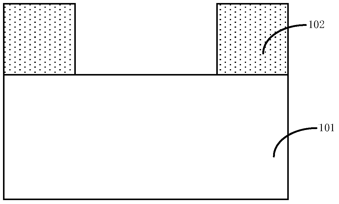
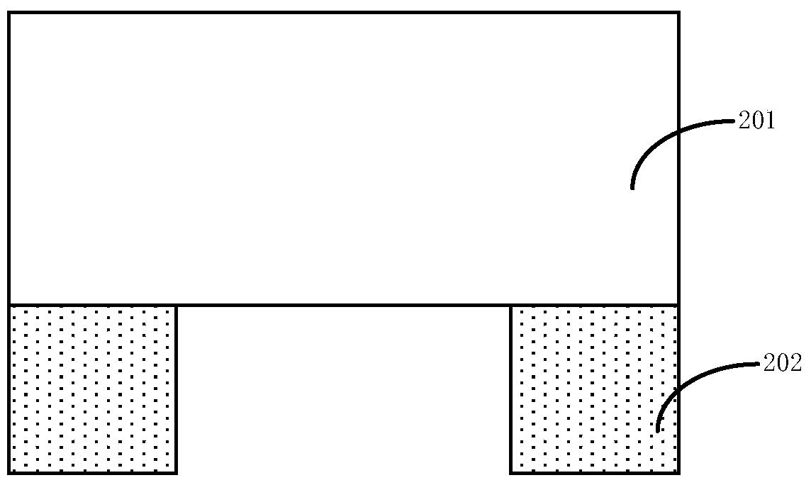
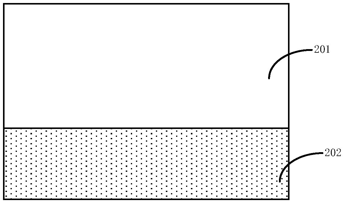
[0051] in figure 1 is a structural schematic diagram of the element wafer; Figure 2a-2b is a structural schematic diagram of the supporting wafer; Figure 2c A structural schematic diagram of unbonding the element wafer and the support wafer; image 3 It is a flow chart of the manufacturing process of the semiconductor device described in a specific embodiment of the present invention.

[0052] First, step 201 is performed to provide an element wafer 101 , a first bonding interface layer 102 is formed on the front surface of the element wafer, and a first cavity is formed in the first bonding interface layer 102 .

[0053] Specifically, such as figure 1 Said, components and interconnection structures, such as metal pads, are formed in the component...

Embodiment 2

[0092] The present invention also provides a semiconductor device, which is prepared by the method described in Embodiment 1. The semiconductor device prepared by the method described in Embodiment 1 of the present invention is lower in price, and has higher yield and yield.

Embodiment 3

[0094] The present invention also provides an electronic device, including the semiconductor device described in Embodiment 2. Wherein, the semiconductor device is the semiconductor device described in Embodiment 2, or the semiconductor device obtained according to the preparation method described in Embodiment 1.

[0095] The electronic device of this embodiment can be any electronic product or equipment such as mobile phone, tablet computer, notebook computer, netbook, game console, TV set, VCD, DVD, navigator, camera, video recorder, voice recorder, MP3, MP4, PSP, etc. , can also be any intermediate product including the semiconductor device. The electronic device according to the embodiment of the present invention has better performance due to the use of the above-mentioned semiconductor device.


PUM


Abstract

The invention relates to a semiconductor device, a preparation method thereof and an electronic device with the semiconductor device. The preparation method comprises the steps of S1, providing a component wafer of which the front surface is provided with a first bonding interface layer, and furthermore a first chamber is formed in the first bonding interface layer; S2, providing a supporting wafer on which a second bonding interface layer is formed; S3, bonding the first bonding interface layer with the second bonding interface layer, thereby integrating the component wafer and the supporting wafer; S4, grinding the back surface of the component wafer; and S5, de-bonding the component wafer and the supporting wafer in a mechanical method, thereby separating the component wafer from the supporting wafer. The preparation method of the semiconductor device has advantages of realizing simpler operation, greatly reducing process cost and improving process yield.

Description

technical field [0001] The present invention relates to the field of semiconductors, in particular, the present invention relates to a semiconductor device, a preparation method thereof, and an electronic device. Background technique [0002] In semiconductor technology, many products currently require thin wafer (waferthickness<=400um) processing methods. For example, in 3DIC three-dimensional stacking technology, the popular 3D through-silicon via (TSV) process, 2.5D interposer (Interposer) process, insulated gate bipolar transistor process (InsulatedGateBipolarTransistor, IGBT), and backside illumination (BSI) process are all There is a need for a method of processing such flakes. [0003] At present, there are two kinds of wafer processing methods: one is the Taiko wafer (Wafer) method of Disco; the Taiko grinding process is one of the grinding methods of thin silicon wafers, which is characterized in that only the central part of the silicon wafer is ground, and the...

Claims


Application Information

Patent Timeline
IPC IPC(8): H01L21/683
Inventor 陈福成黄河向阳辉施林波
Owner SEMICON MFG INT (SHANGHAI) CORP
Why Eureka
Eureka Blog
Learn More