Supercharge Your Innovation With Domain-Expert AI Agents!

A kind of preparation method of light-emitting diode

A technology of light-emitting diodes and electrodes, which is applied in semiconductor/solid-state device manufacturing, semiconductor devices, electrical components, etc., can solve the problems of low cutting efficiency and high production cost, and achieve the effect of improving cutting efficiency and reducing production cost

Active Publication Date: 2019-02-05
HC SEMITEK SUZHOU
View PDF5 Cites 0 Cited by
  • Summary
  • Abstract
  • Description
  • Claims
  • Application Information

AI Technical Summary

Problems solved by technology

[0006] In order to solve the problems of low cutting efficiency and high production cost in the prior art, an embodiment of the present invention provides a method for preparing a light-emitting diode

Method used


Image

  • A kind of preparation method of light-emitting diode
  • A kind of preparation method of light-emitting diode
  • A kind of preparation method of light-emitting diode

Examples


Embodiment 1

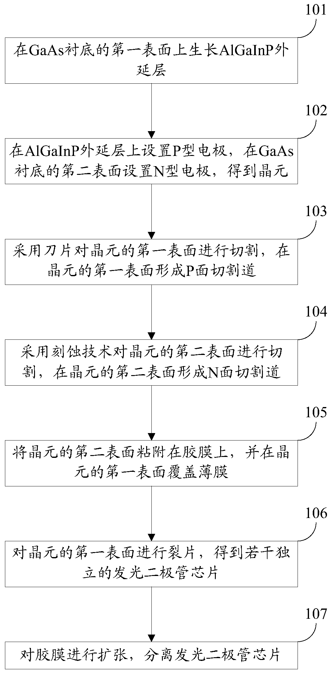
[0043] The embodiment of the present invention provides a method for preparing a light-emitting diode, see figure 1 , the preparation method comprises:

[0044] Step 101: growing an AlGaInP epitaxial layer on the first surface of the GaAs substrate.

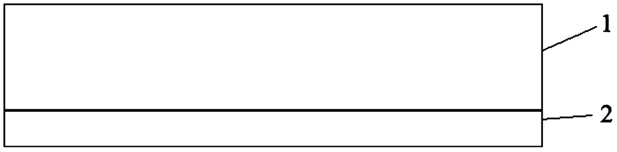
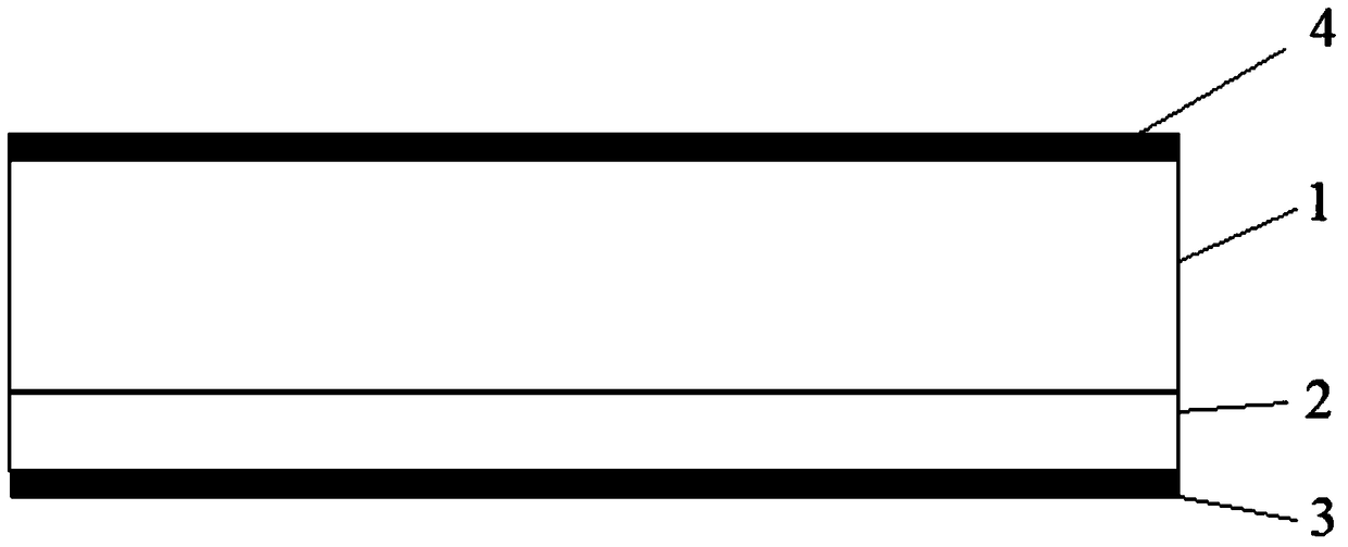
[0045] Figure 2a It is a schematic structural diagram of the light emitting diode after step 101 is executed. Among them, 1 is the GaAs substrate, and 2 is the AlGaInP epitaxial layer.

[0046] In this embodiment, the AlGaInP epitaxial layer may include an N-type AlInP confinement layer sequentially stacked on a GaAs substrate, two alternately stacked AlGaInP multiquantum well layers with different Al compositions, and a P-type AlInP confinement layer.

[0047] Specifically, this step 101 may include:

[0048] An AlGaInP epitaxial layer is grown on the first surface of the GaAs substrate by using Metal-organic Chemical Vapor Deposition (MOCVD for short) technology.

[0049] Step 102: setting a P-type electrode on the AlGaIn...

Embodiment 2

[0102] The embodiment of the present invention provides a method for preparing a light-emitting diode, see Figure 5 , the preparation method comprises:

[0103] Step 201: growing an AlGaInP epitaxial layer on the first surface of the GaAs substrate.

[0104] Figure 6a It is a schematic structural diagram of the light emitting diode after step 201 is executed. Among them, 1 is the GaAs substrate, and 2 is the AlGaInP epitaxial layer.


PUM

PropertyMeasurementUnit
widthaaaaaaaaaa
depthaaaaaaaaaa
depthaaaaaaaaaa

Abstract

The invention discloses a preparation method of an LED, and belongs to the technical field of semiconductors. The preparation method comprises the following steps: growing an AlGaInP epitaxial layer on the first surface of a GaAs substrate; setting a P-type electrode on the AlGaInP epitaxial layer and setting an N-type electrode on the second surface of the GaAs substrate to obtain a wafer; cutting the first surface of the wafer to form a P-surface cutting gap in the first surface of the wafer; cutting the second surface of the wafer by using an etching technology to form an N-surface cutting gap in the second surface of the wafer; adhering the second surface of the wafer onto an adhesive film, and enabling the first surface of the wafer to be covered with a thin film; splitting the first surface of the wafer to obtain a plurality of independent LED chips; and expanding the adhesive film to separate the LED chips. According to the preparation method, cutting is carried out by using the etching technology on at least one surface, so that the cutting efficiency is greatly improved, and the production cost is reduced.

Description

technical field [0001] The invention relates to the technical field of semiconductors, in particular to a method for preparing a light emitting diode. Background technique [0002] As the most eye-catching new-generation light source in the world, Light Emitting Diode (LED for short) is known as the most promising LED in the 21st century due to its advantages of high brightness, low heat, long life, non-toxicity, and recyclability. Development prospects of green lighting sources. Among them, AlGaInP light-emitting diodes have excellent performance in yellow-green, orange, orange-red, and red bands, and are widely used in white light sources, full-color displays, traffic lights, and urban lighting projects. [0003] The preparation method of AlGaInP light-emitting diodes includes: growing an AlGaInP epitaxial layer on the first surface of a GaAs substrate; setting a P-type electrode on the AlGaInP epitaxial layer, and setting an N-type electrode on the second surface of the ...

Claims


Application Information

Patent Timeline
Patent Type & Authority Patents(China)
IPC IPC(8): H01L33/00H01L21/78
CPCH01L21/78H01L33/0095
Inventor 肖千宇高本良薛蕾常远林晓文卞广彪葛丁壹王梦杰陈晞
Owner HC SEMITEK SUZHOU
Features
  • R&D
  • Intellectual Property
  • Life Sciences
  • Materials
  • Tech Scout
  • Unparalleled Data Quality
  • Higher Quality Content
  • 60% Fewer Hallucinations
Learn More