NFC antenna integrated on ferrite and preparation method thereof

A technology of ferrite and ferrite layer, applied in the direction of antenna support/mounting device, radiation element structure, etc., can solve the problems of low production efficiency, long processing cycle, thick thickness, etc., and achieve high production efficiency and high product quality. Thin, save the effect of lamination process

Inactive Publication Date: 2016-05-11
SHANGHAI LINEPRINTING MATERIALS CO LTD
View PDF4 Cites 2 Cited by
  • Summary
  • Abstract
  • Description
  • Claims
  • Application Information

AI Technical Summary

Problems solved by technology

[0003] see figure 1 As shown, the antenna is generally composed of a circuit board and ferrite materials with anti-interference ability. The traditional NFC antenna manufacturing method usually uses the circuit board and the ferrite substrate to be processed separately, and the circuit board needs to go through drilling-black hole-plating Copper-film-exposure-developing-etching-removing-film-printing-gold plating and other series of processing steps are formed, and then combined with the formed ferrite substrate to form a module, so the processing cycle is relatively long, the thickness is thick, and the production Defects such as low efficiency

Method used


Image

  • NFC antenna integrated on ferrite and preparation method thereof
  • NFC antenna integrated on ferrite and preparation method thereof
  • NFC antenna integrated on ferrite and preparation method thereof

Examples


Embodiment Construction

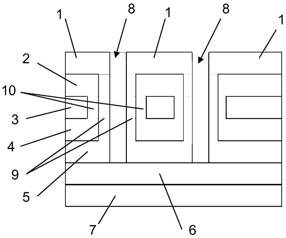
[0025] The NFC antenna integrated on the ferrite of the present invention is as figure 1 As shown, it includes the first electroplated copper layer 1, the first catalytic ink layer 2, the ferrite layer 3, the second catalytic ink layer 4, the second electroplated copper layer 5, the solder resist ink layer 6, Double-sided adhesive layer 7, and several longitudinal holes 8 are also provided on the antenna. The upper end of the longitudinal hole 8 is opened on the upper surface of the first electroplated copper layer 1, and the lower end is on the upper surface of the solder resist ink layer 6, and the two sides of the longitudinal hole 8 are from the outside. The third electroplated copper layer 9 and the third catalytic ink layer 10 are sequentially included in the inner lateral direction, and the third electroplated copper layer 9 is connected with the first and second electroplated copper layers 1 and 5, and the third electroplated copper layer 10 is connected with the first ...


PUM


Abstract

The invention discloses an NFC antenna integrated on ferrite and a preparation method thereof. Through drilling on the ferrite, the front surface and the back surface of the ferrite are communicated. Then catalyzed ink printing and copper electroplating are performed on the front surface and the back surface of the ferrite, and solder mask is printed for protecting a line. Because NFC is directly implanted on the ferrite, production efficiency is greatly improved and an efficiency advantage is realized. Furthermore a traditional flexible circuit board manufacturing process and a ferrite adhesion process are saved, thereby realizing a cost advantage. Furthermore smaller thickness of an NFC product can be realized, thereby further reducing the mechanism space of a client and obtaining smaller thickness of the product.

Description

technical field [0001] The invention belongs to an antenna preparation process, and in particular relates to an NFC antenna integrated on a ferrite and a preparation method thereof. Background technique [0002] The NFC antenna is a component used to transmit or receive electromagnetic waves in a radio device. It replaces the guided wave propagating on the transmission line with an electromagnetic wave propagating in an unbounded medium (usually free space), or vice versa. Engineering systems such as radio communication, broadcasting, television, radar, navigation, electronic countermeasures, remote sensing, and radio astronomy, which use electromagnetic waves to transmit information, rely on antennas to work. In addition, in terms of transmitting energy with electromagnetic waves, non-signal energy radiation also requires antennas. [0003] see figure 1 As shown, the antenna is generally composed of a circuit board and ferrite materials with anti-interference ability. The...

Claims


Application Information

Patent Timeline
Patent Type & Authority Applications(China)
IPC IPC(8): H01Q1/38H01Q1/22
Inventor 杨恺苏临萍刘春雷徐厚嘉陈冠霖
Owner SHANGHAI LINEPRINTING MATERIALS CO LTD
Why Eureka
Try Eureka