Eureka AIR delivers breakthrough ideas for toughest innovation challenges, trusted by R&D personnel around the world.

Charge pump circuit for low power supply voltage condition

A low power supply voltage, charge pump technology, applied in the direction of conversion equipment without intermediate conversion to AC, can solve the problems of complex power system, device isolation and ESD protection design difficulty, etc., to reduce fluctuations and eliminate substrates Bias effect, the effect of stable and reliable operation

Inactive Publication Date: 2016-05-11
SHANGHAI HUAHONG INTEGRATED CIRCUIT
View PDF5 Cites 0 Cited by
  • Summary
  • Abstract
  • Description
  • Claims
  • Application Information

AI Technical Summary

Problems solved by technology

In many systems using charge pumps, the dual power supply mode has to be used to solve the above contradictions. However, the dual power supply makes the power system of the chip more complicated, and the power network design, device isolation and ESD protection design are more difficult.

Method used


Image

  • Charge pump circuit for low power supply voltage condition
  • Charge pump circuit for low power supply voltage condition

Examples


Embodiment Construction

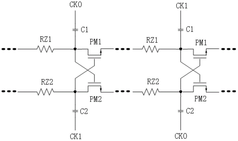
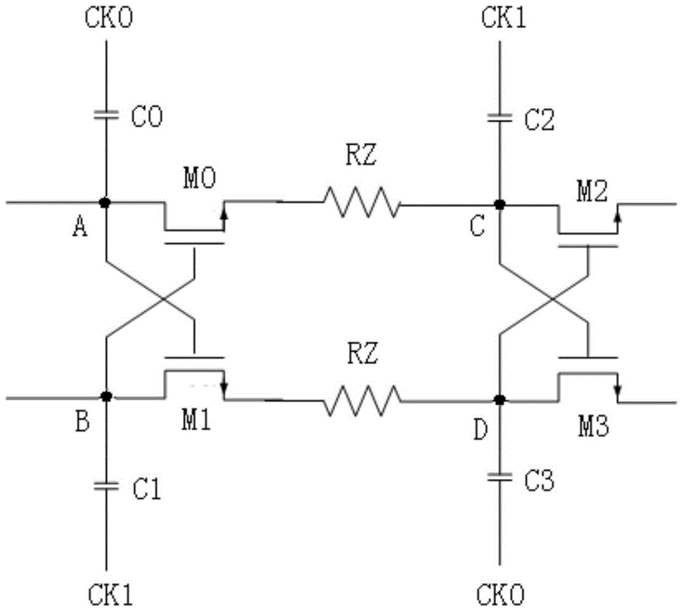
[0011] see figure 1 As shown, the charge pump circuit used under the condition of low power supply voltage is composed of cascaded multi-stage circuits; each stage circuit includes two resistors, two capacitors and two PMOS transistors; one end of the first resistor RZ1 is connected to One end of the first capacitor C1, the drain of the first PMOS transistor PM1 and the gate of the second PMOS transistor PM2 are connected; one end of the second resistor RZ2 is connected to one end of the second capacitor C2, the drain of the second PMOS transistor PM2 and The gate of the first PMOS transistor PM1 is connected. Since the substrate of the PMOS transistor can be connected to the source of the PMOS transistor, there is no problem of threshold voltage rise caused by the substrate bias effect after the voltage rises, thus ensuring that the charge transfer efficiency will not deteriorate sharply with the rise of the output voltage . The low power supply voltage refers to less than ...


PUM


Abstract

The invention discloses a charge pump circuit for a low power supply voltage condition. A plurality of levels of circuits are cascaded to form the charge pump circuit; each level of circuit includes two resistors, two capacitors and two PMOS transistors, wherein one end of the first resistor is connected with one end of the first capacitor, the drain of the first PMOS transistor is connected with the gate of the second PMOS transistor, and one end of the second resistor is connected with one end of the second capacitor, the drain of the second PMOS transistor is connected with the gate of the first PMOS transistor. The charge pump circuit of the invention can work stably and reliably under the low power supply voltage condition.

Description

technical field [0001] The invention relates to a charge pump circuit. In particular, it relates to a charge pump circuit for low supply voltage conditions. Background technique [0002] With the continuous improvement of semiconductor manufacturing technology and integrated circuit design capabilities, people have been able to integrate processors, memory, analog circuits, interface logic and even radio frequency circuits into one chip, which is the System-on-Chip (System-on-Chip, SoC). As the data throughput continues to rise and the system requires low power consumption, the SoC core voltage (corevdd) is gradually reduced. Currently, the core voltage of an SoC system is generally below 1.8V, and it is foreseeable that it will be further reduced to 1.5V or even 1.2V in the near future. This brings great challenges to the design of analog circuits, especially circuits that are sensitive to power supply voltage, such as charge pump circuits. In many systems that use char...

Claims


Application Information

Patent Timeline
Patent Type & Authority Applications(China)
IPC IPC(8): H02M3/07
Inventor 夏天
Owner SHANGHAI HUAHONG INTEGRATED CIRCUIT
Why Eureka
Eureka Blog
Learn More