Substrates And Integrated Circuit Chip With Improved Pattern

A technology of integrated circuits and patterns, applied in circuits, electrical components, electrical solid devices, etc., can solve problems such as short circuits, achieve the effects of improving withstand voltage characteristics, effective thermal control, and reducing the incidence of defects

Inactive Publication Date: 2016-05-18
SILICON WORKS CO LTD
View PDF1 Cites 0 Cited by
  • Summary
  • Abstract
  • Description
  • Claims
  • Application Information

AI Technical Summary

Problems solved by technology

[0010] When a high voltage is momentarily applied to a high-voltage terminal, a strong electric field is momentarily generated between the high-voltage terminal and adjacent terminals, resulting in the following problems: between the high-voltage terminal and adjacent terminals, between the high-voltage terminal Increased possibility of short circuit between the body land and the high-voltage terminal pattern on the substrate corresponding to the high-voltage terminal and an adjacent pattern, or between the high-voltage terminal pattern and the body pattern

Method used


Image

  • Substrates And Integrated Circuit Chip With Improved Pattern
  • Substrates And Integrated Circuit Chip With Improved Pattern
  • Substrates And Integrated Circuit Chip With Improved Pattern

Examples


Embodiment Construction

[0043] Hereinafter, embodiments of the present invention will be described in detail with reference to the accompanying drawings. In the following description, detailed descriptions of known elements or functions that may make the gist of the invention unnecessarily unclear will be omitted.

[0044] However, the present invention is not limited to or limited by these embodiments. Throughout the drawings, the same reference characters designate the same parts.

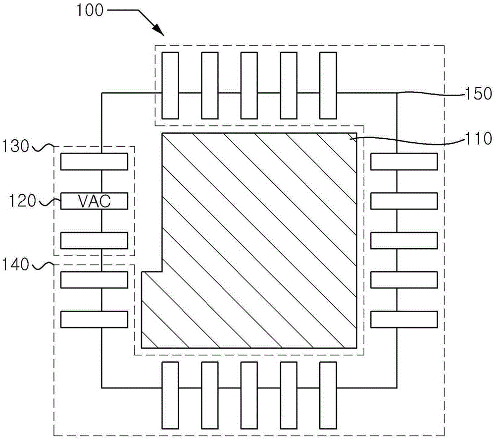
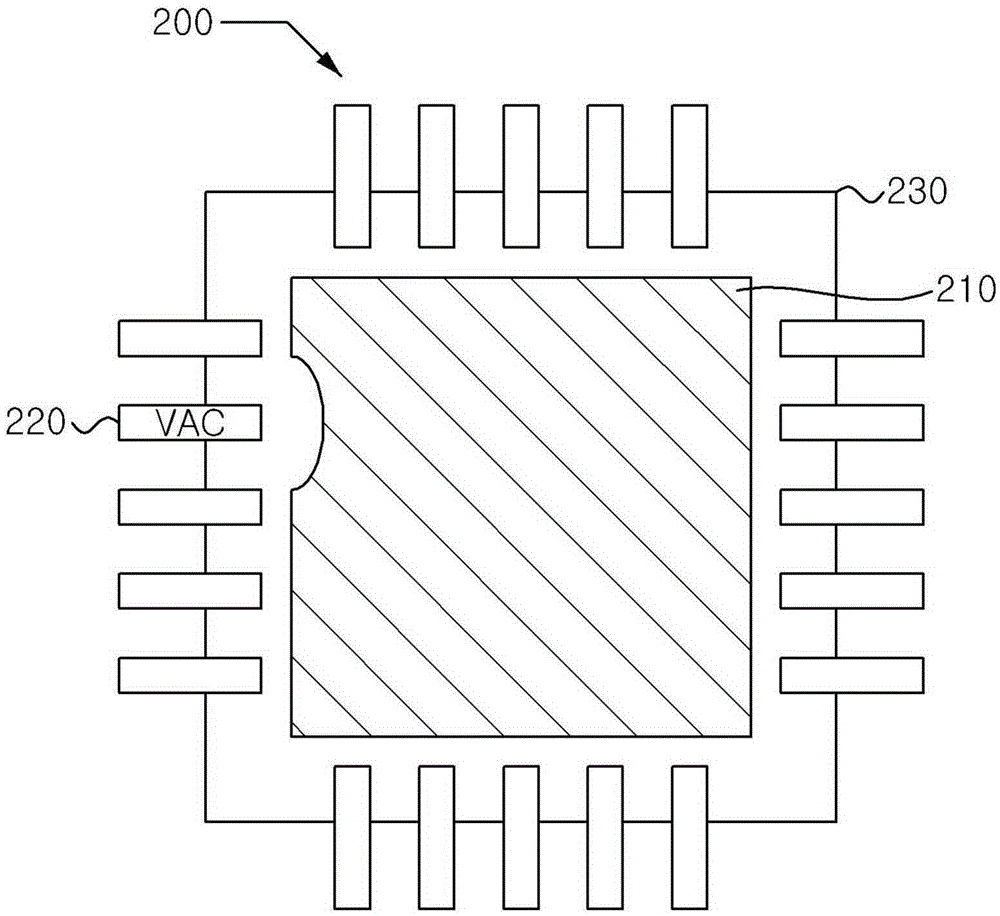
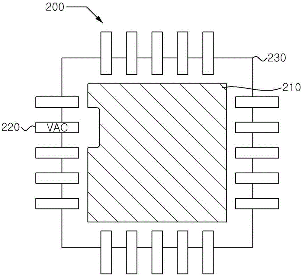
[0045] figure 1 is a diagram illustrating a substrate according to an embodiment of the present invention, in which a region including a terminal to which a high voltage is applied and a body pattern are separated by a distance.

[0046] The packaging substrate is a type of printed circuit board (PCB). Package substrates can be used as core semiconductors for mobile devices and PCs. The packaging substrate can carry electrical signals between the semiconductor and the motherboard. The substrate may be a high-densit...


PUM


Abstract

The present invention relates to a substrate and integrated circuit chip with improved patterns, and more particularly to technology that is efficient in terms of thermal control and that can reduce the causes of occurrence of defects during the operation of a terminal to which a high voltage is applied. The present invention is characterized in that a first clearance distance between a first terminal, to which a voltage higher than voltages to be applied to the remaining terminals is applied, or first terminal pattern corresponding to the first terminal and a body pattern present between an integrated circuit chip and a substrate is larger than a second clearance distance between a second terminal, including at least some of the remaining terminals other than the first terminal, or second terminal pattern corresponding to the second terminal and the body pattern.

Description

[0001] Cross References to Related Applications [0002] This application claims the benefit of Korean Application No. 10-2014-0153841 filed on November 6, 2014, which is incorporated herein by reference. technical field [0003] The present invention relates to package substrates and integrated circuit chips having improved patterns, and more particularly, to techniques effective in thermal control and capable of reducing causes of defects generated during operation of terminals to which high voltage is applied. Background technique [0004] In an effort to save energy, lighting technologies using light emitting diodes (LEDs) as light sources have been being developed. In particular, high brightness LEDs have advantages over other light sources due to various factors such as energy consumption, lifetime, and quality of illumination. [0005] A problem with a lighting device using such an LED as a light source is that, due to characteristics of the LED, the LED can generate...

Claims


Application Information

Patent Timeline
Patent Type & Authority Applications(China)
IPC IPC(8): H01L23/48H01L23/488H01L23/498H01L23/367
CPCH01L23/367H01L23/48H01L23/488H01L23/49838H01L23/49541H01L24/05H01L24/06H01L33/62H01L33/642H01L2224/0401H01L2224/04026H01L2224/05552H01L2224/0603H01L2224/06051H01L2224/0615H01L2224/06177H01L2224/131H01L2224/16227H01L2224/291H01L2224/32227H01L2224/73103H01L2224/73203H01L2224/81815H01L2224/83192H01L2224/83815H01L2924/14H01L2924/301H01L2924/00012H01L2924/00014H01L2924/014
Inventor 李相永文耿植安基哲
Owner SILICON WORKS CO LTD
Why Eureka
Try Eureka