Terminal protection structure of super junction device and manufacturing method of terminal protection structure

A terminal protection structure, super junction technology, applied in semiconductor/solid-state device manufacturing, electrical solid-state devices, semiconductor devices and other directions, can solve different problems

Active Publication Date: 2012-04-18
SHANGHAI HUAHONG GRACE SEMICON MFG CORP
View PDF4 Cites 13 Cited by
  • Summary
  • Abstract
  • Description
  • Claims
  • Application Information

AI Technical Summary

Problems solved by technology

[0003] For existing devices such as high-voltage VDMOS, there are diffusion guard ring technologies and field plate technologies such as floating field plate technology, resistive field plate technology, equipotential ring technology, field limiting ring technology, junct

Method used


Image

  • Terminal protection structure of super junction device and manufacturing method of terminal protection structure
  • Terminal protection structure of super junction device and manufacturing method of terminal protection structure
  • Terminal protection structure of super junction device and manufacturing method of terminal protection structure

Examples


Embodiment Construction

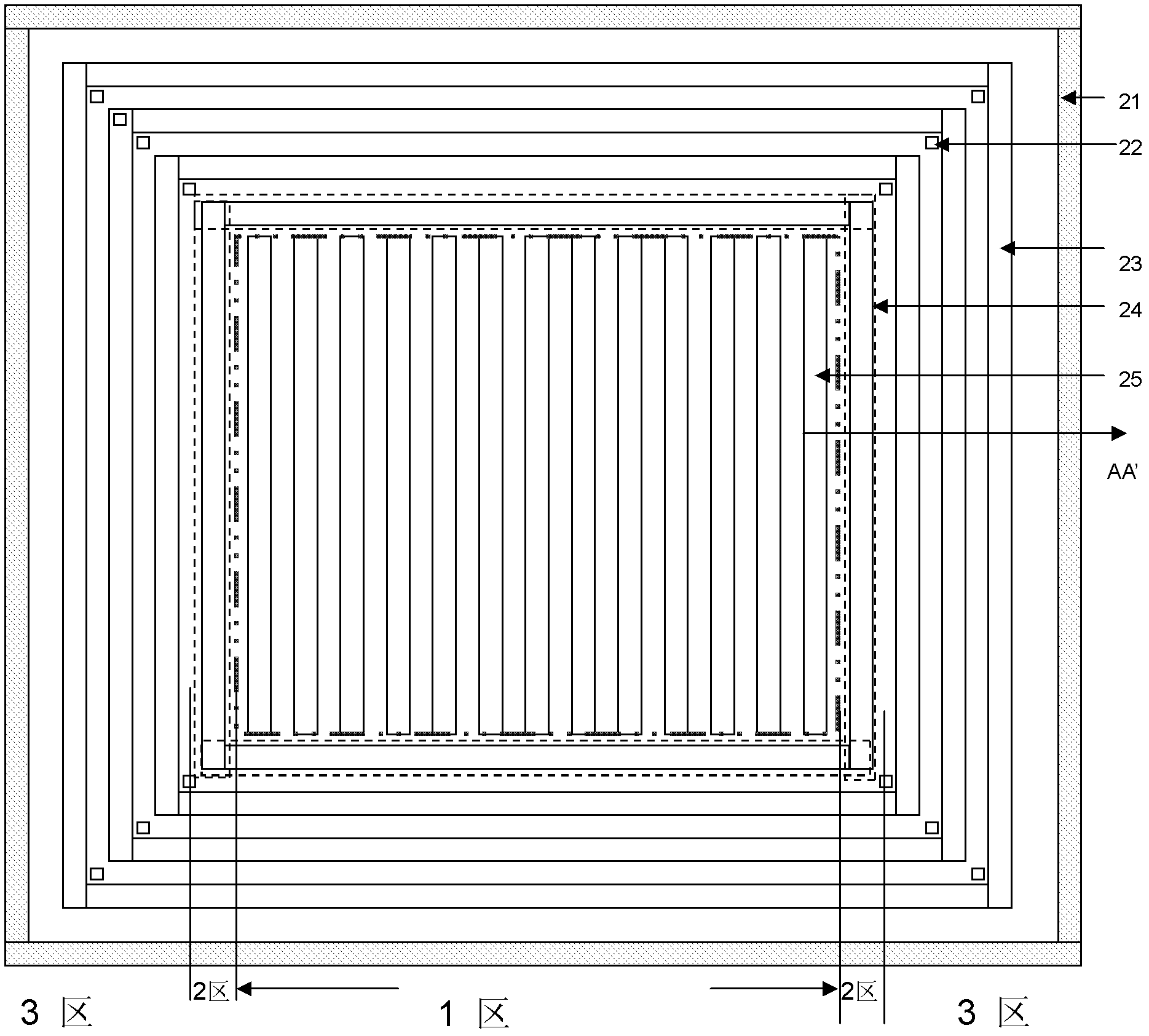
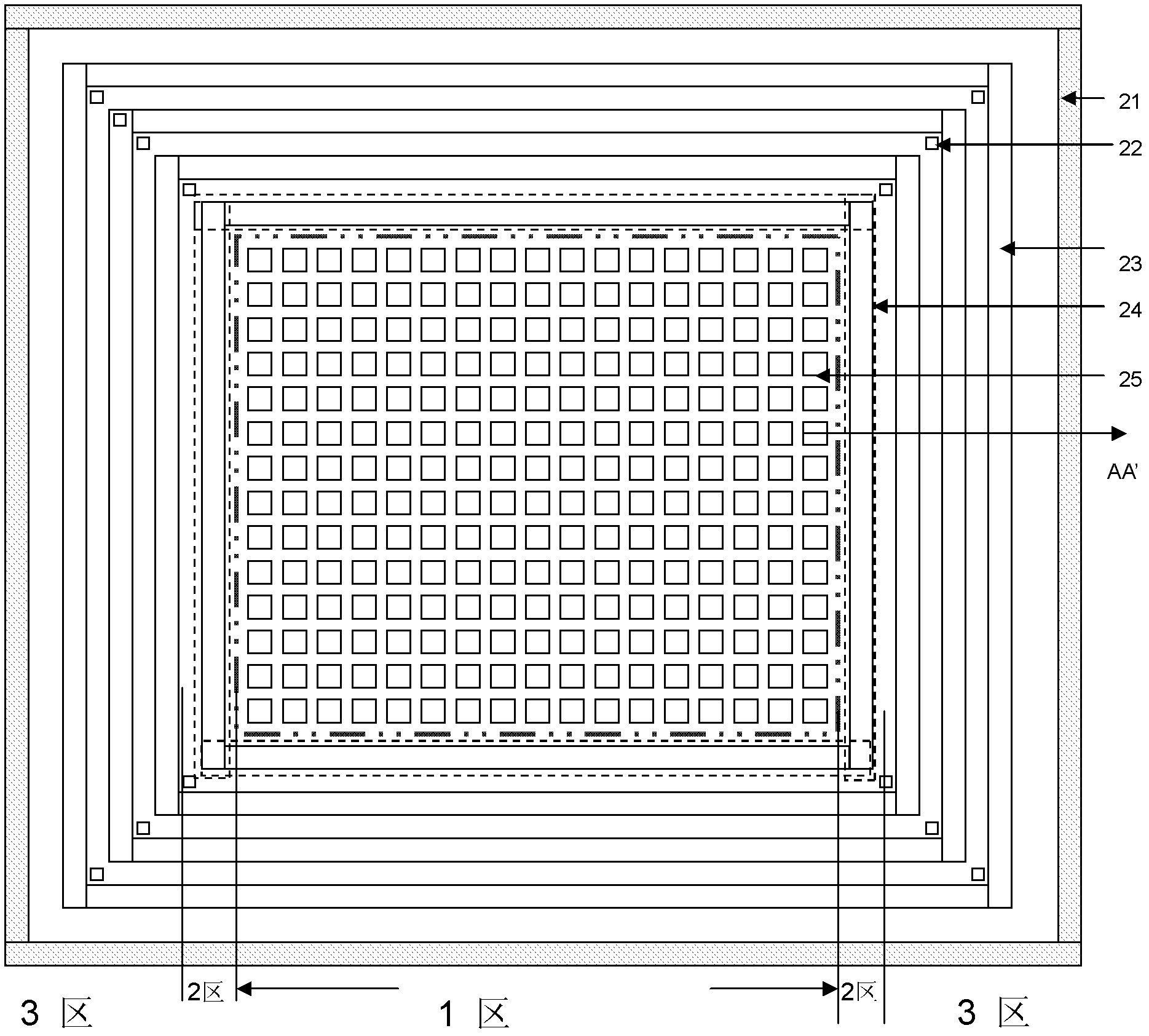
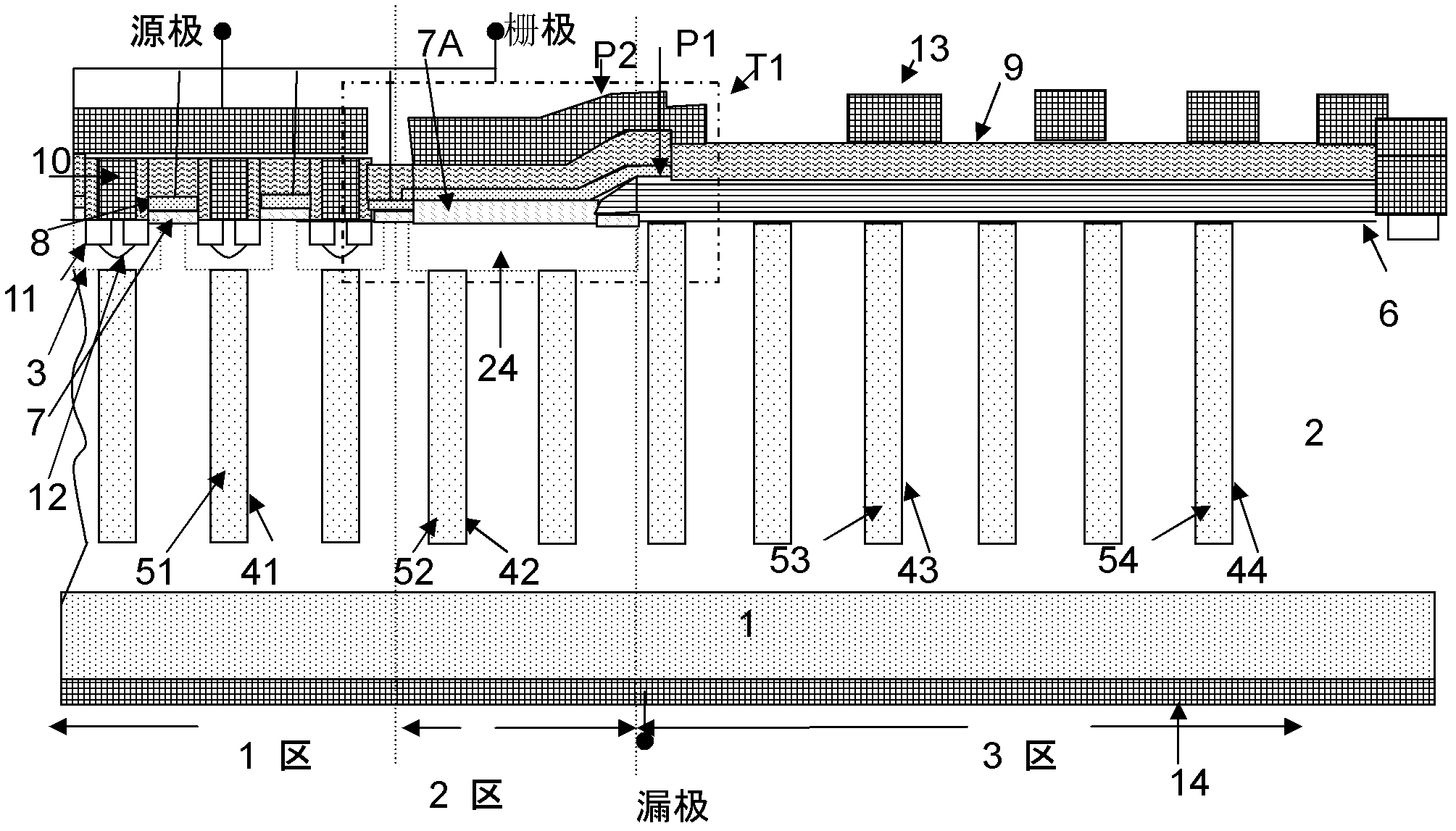
[0063] Such as figure 1 As shown, it is a top view of the terminal protection structure of the super junction device according to the embodiment of the present invention Figure 1 . In the top view, the embodiment of the present invention can be divided into zone 1, zone 2 and zone 3. Region 1 is the middle region of the super junction device is the current flow region, and the current flow region includes alternately arranged P-type regions 25 and N-type regions formed in the N-type silicon epitaxial layer; in the current flow region, the current It will pass through the N-type region from the source to the drain through the channel, and the P-type region 25 is in a reverse cut-off state and forms a depletion region together with the N-type region to withstand voltage. Regions 2 and 3 are the terminal protection structure regions of the super junction device. The terminal protection structure does not provide current when the device is turned on, and is used to bear the per...


PUM

PropertyMeasurementUnit
Tilt angleaaaaaaaaaa

Abstract

The invention discloses a terminal protection structure of a super junction device, which adopts a combined structure of a polycrystalline silicon field plate and a metal field plate. One polycrystalline silicon field plate covers a footstep structure of a terminal medium membrane and the polycrystalline silicon field plate is further covered by two medium layers with different thicknesses, so that an electric field on the surface of the device can be alleviated. In the invention, a P-type ring with a higher concentration is kept under the field plate so that a current processing capability of the device is improved when the device is used in an inductive circuit. According to the invention, the structure configuration of a P-type column and an N-type column in the terminal protection structure can assure that the device is turned off when the device is applied to the inductive circuit and the position of generating avalanche-like breakdown in the terminal protection structure is ensured to be close to the front side of a silicon sheet when a current overshoot happens, so that the capability of resisting the overshoot current is improved. The invention further discloses the terminal protection structure of the super junction device and a manufacturing method of the terminal protection structure. According to the terminal protection structure of the super junction device, provided by the invention, the voltage endurance, the current processing capability and the reliability of the device can be improved and the process cost is not increased.

Description

technical field [0001] The invention relates to the field of semiconductor integrated circuit manufacturing, in particular to a terminal protection structure of a super junction device; the invention also relates to a manufacturing method of the terminal protection structure of a super junction device. Background technique [0002] The super junction MOSFET adopts a new voltage-resistant layer structure, and uses a series of alternately arranged P-type semiconductor thin layers and N-type semiconductor thin layers to combine the P-type semiconductor thin layers and N-type semiconductor thin layers at a lower voltage in the off state. The thin layer of semiconductor is depleted to achieve mutual compensation of charges, so that the thin layer of P-type semiconductor and thin layer of N-type semiconductor can achieve high breakdown voltage under high doping concentration, so as to obtain low on-resistance and high breakdown at the same time voltage, breaking the theoretical li...

Claims


Application Information

Patent Timeline
IPC IPC(8): H01L29/06H01L27/02H01L21/336H01L21/82
Inventor 肖胜安
Owner SHANGHAI HUAHONG GRACE SEMICON MFG CORP
Why Eureka
Try Eureka