Automated optical inspection device and method for defect inspection of LCD (liquid crystal display) module

An optical automatic detection and defect detection technology, applied in optics, nonlinear optics, instruments, etc., can solve the problems of parallel image processing, complicated equipment interaction, and long detection time, so as to achieve versatility and reduce interaction complexity , the effect of reducing the overall cost

Inactive Publication Date: 2016-05-25
WUHAN JINGCE ELECTRONICS GRP CO LTD
View PDF5 Cites 37 Cited by
  • Summary
  • Abstract
  • Description
  • Claims
  • Application Information

AI Technical Summary

Problems solved by technology

Image acquisition, PG, and image processing are implemented separately. The equipment interaction is complicated and the cost is high. How

Method used


Image

  • Automated optical inspection device and method for defect inspection of LCD (liquid crystal display) module
  • Automated optical inspection device and method for defect inspection of LCD (liquid crystal display) module

Examples


Embodiment Construction

[0026] The present invention will be further described below in conjunction with the accompanying drawings and examples. Obviously, the examples are only some examples of the present invention, not all examples, so the examples should not be construed as limiting the present invention.

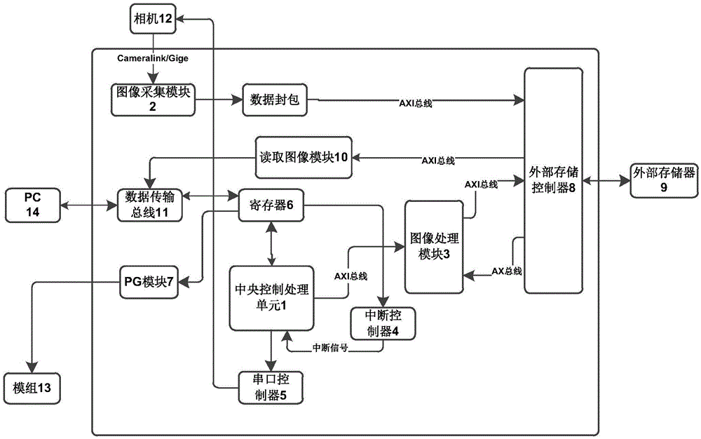
[0027] Such as figure 1 As shown, the optical automatic detection device used for LCD liquid crystal module defect detection in the present invention includes: a central control processing unit 1 integrated in the FPGA, an image acquisition module 2, an image processing module 3, an interrupt controller 4, and a serial port controller 5 , register 6, PG module 7, external storage controller 8, read image module 10, data transmission bus 11 and external storage module 9 outside FPGA, camera 12, module 13 and PC personal computer 14. Wherein, the data transmission bus 11 adopts a PCIE bus.

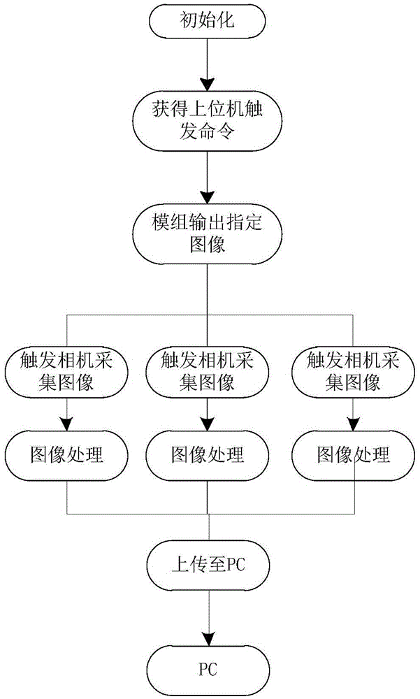
[0028] Such as figure 2 Be the optical automatic detection method that the present invention is used f...


PUM


Abstract

The invention relates to the technical field of automated optical inspection of LCD (liquid crystal display) modules, in particular to an automated optical inspection device for defect inspection of an LCD module and an automated optical inspection method for the defect inspection of the LCD module. The device comprises a central control processing unit, an image acquisition module, an image processing module and a PG (Pattern Generate) module. The method comprises the following steps of receiving a PG configuration parameter and a camera configuration parameter, lighting up modules according to the PG configuration parameter, configuring a camera according to the camera configuration parameter, controlling the camera to shoot an module image and collect the shot image, performing image processing and defect inspection on the collected original image, and outputting a defect inspection result and processed image data. The device and the method provided by the invention have the advantages that the image acquisition module, the PG module and the image processing module are integrated on an FPGA (Field Programmable Gate Array), and the whole testing process is performed based on the FPGA, so that the system integration degree is improved, the interaction complexity is lowered, the real-time processing performance is improved, the defect inspection time is shortened, the system stability is greatly improved, the inspection time is shortened, and the factory production efficiency is improved.

Description

technical field [0001] The invention relates to the technical field of automatic optical detection of liquid crystal modules, in particular to an optical automatic detection device and method for defect detection of LCD liquid crystal modules. Background technique [0002] In the field of automatic optical inspection (AOI) of liquid crystal modules, several modules or devices such as image acquisition, PG (PatternGenerate-pattern generation equipment) and image processing are involved. The traditional AOI design method is to realize these three parts separately. : The host computer controls the independent PG to generate the required test image, and then collects the image through the existing image acquisition card on the market, and finally transmits it to the PC through the PCIE bus, and then the PC performs image defect detection. [0003] A separate PG is configured exclusively for generating test screens, which is not conducive to system integration and system coordina...

Claims


Application Information

Patent Timeline
IPC IPC(8): G02F1/13G09G3/00
CPCG02F1/1309G09G3/006
Inventor 简平超欧昌东梅林海汪舟董文忠
Owner WUHAN JINGCE ELECTRONICS GRP CO LTD
Why Eureka
Try Eureka