Electrochromic device for screening solid inorganic electrochromic materials at high throughput and manufacturing method of electrochromic device

A technology of electrochromic devices and electrochromic materials, applied in instruments, nonlinear optics, optics, etc., can solve the problems of cumbersome operation, high technical difficulty, large error, etc., and achieve improved work efficiency, simple operation, and small error Effect

Active Publication Date: 2016-05-25
CHINA BUILDING MATERIALS ACAD
View PDF4 Cites 5 Cited by
  • Summary
  • Abstract
  • Description
  • Claims
  • Application Information

AI Technical Summary

Problems solved by technology

[0004] When researchers use high-throughput screening technology to screen materials with the best color-changing effect or light transmittance from single-component electrochromic materials, they generally use different thicknesses of electrochromic material film layers to verify and screen. Different thicknesses of the layers have different color-changing effects and light transmittance. Researchers can select the electrochromic material with the optimal thickness by verifying its color-changing effect and light transmittance. However, the electrochromic material film layer prepared by the existing technology There are fewer types of thickness, and it is impossible to prepare electrochromic materials with more thickness types, smaller thickness differences, and simple and accurate preparation methods, so that the optimal thickness of electrochromic materials selected by high-throughput technology is not true. precise;
[0005] Especially for the application of more multi-element doping and composite electrochromic materials, in order to screen out the optimal composition ratio of electrochromic materials and improve the development rate of electrochromic devices, the existing technology uses the configured Solutions with different concentrations are dried to prepare composite electrochromic materials with different formulations. This method has the following problems: to obtain multi-component doped materials, it is necessary to configure a variety of solutions with different concentrations. The composition of inorganic electrochromic materials prepared using the above solutions There are few types of component ratios, which may affect the authenticity of the screening results due to the omission of the optimal content of doping components; to obtain multiple types of formulas, the technical difficulty is high, the operation is cumbersome, and the error is large; The preparation of low-content substances in heterogeneous materials is easy to affect the accuracy of test results due to preparation errors, and also limits the research on the preparation of multi-component doped materials from insoluble substances;
[0006] In summary, there is a same technical problem in the preparation of single-component electrochromic materials or multi-component doped and composite electrochromic materials, that is, it is difficult to prepare various types of electrochromic materials using existing technologies The optimal electrochromic material is obtained for screening by high-throughput technology, and the optimal material selected from fewer types of electrochromic materials by high-throughput technology is not true and inaccurate

Method used


Image

  • Electrochromic device for screening solid inorganic electrochromic materials at high throughput and manufacturing method of electrochromic device
  • Electrochromic device for screening solid inorganic electrochromic materials at high throughput and manufacturing method of electrochromic device
  • Electrochromic device for screening solid inorganic electrochromic materials at high throughput and manufacturing method of electrochromic device

Examples


Embodiment 1

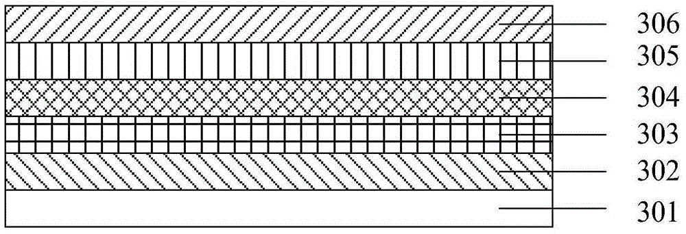
[0041] The glass substrate 301 that surface is deposited with indium oxide tin-doped thin film (lower transparent conductive layer 302) is fixed on the sample holder in the vacuum chamber of magnetron sputtering instrument; Wherein, the glass substrate 301 that surface is deposited with indium oxide tin-doped thin film It can be purchased externally, or the indium oxide tin-doped target can be selected to be plated on the surface of the glass substrate 301 by magnetron sputtering. In this embodiment, it is purchased directly for the convenience of the experiment; first substrate;

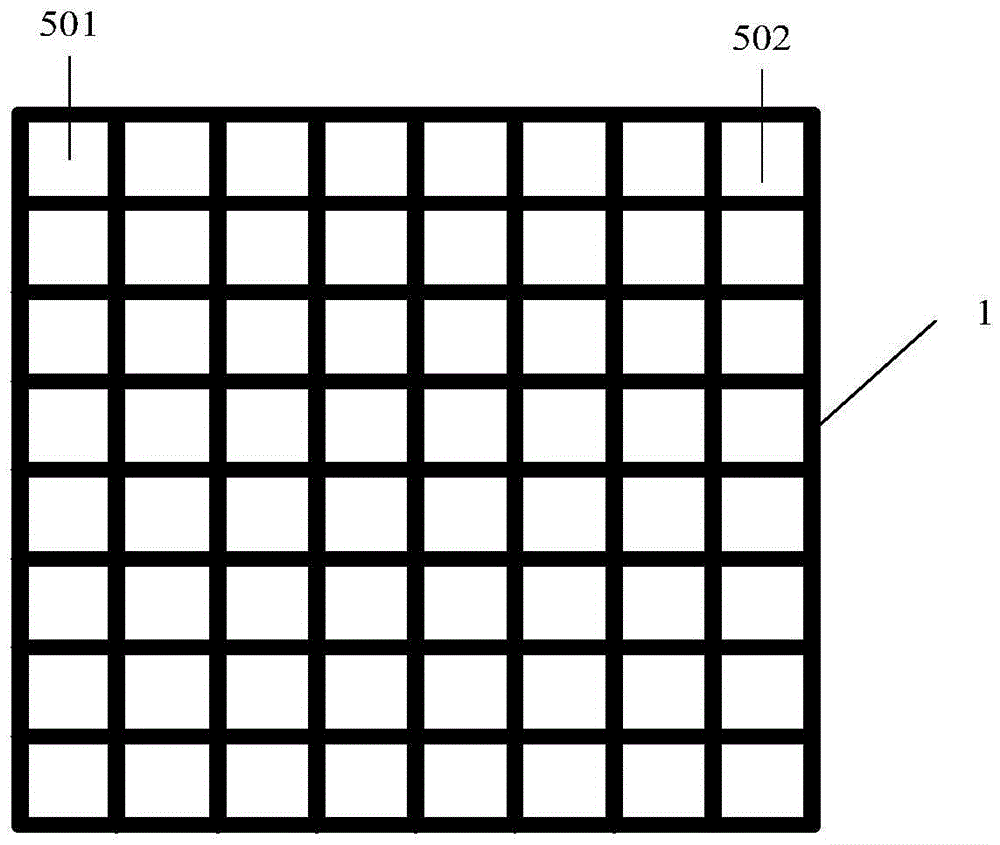
[0042] A polyimide tape is selected as the mask 1. The mask 1 has hollow cells arranged in a matrix of eight rows and eight rows. Each cell is separated by a non-conductive mask 1 and a distance of 2mm is generated. The length and width of each hollowed-out unit cell are 5×5mm, and the above-mentioned mask 1 is covered on the surface of the above-mentioned first substrate, the size of the mask 1 is ...

Embodiment 2

[0058] The glass substrate whose surface is deposited with indium oxide tin-doped film (lower transparent conductive layer) is fixed on the sample holder in the vacuum chamber of the magnetron sputtering instrument; wherein, the glass substrate whose surface is deposited with indium oxide tin-doped film can be directly external You can also choose an indium oxide-doped tin target, and use magnetron sputtering to plate it on the surface of the glass substrate. In this embodiment, it is directly purchased for the convenience of the experiment; the glass substrate with the indium oxide-doped tin film on the surface is used as the first substrate ;

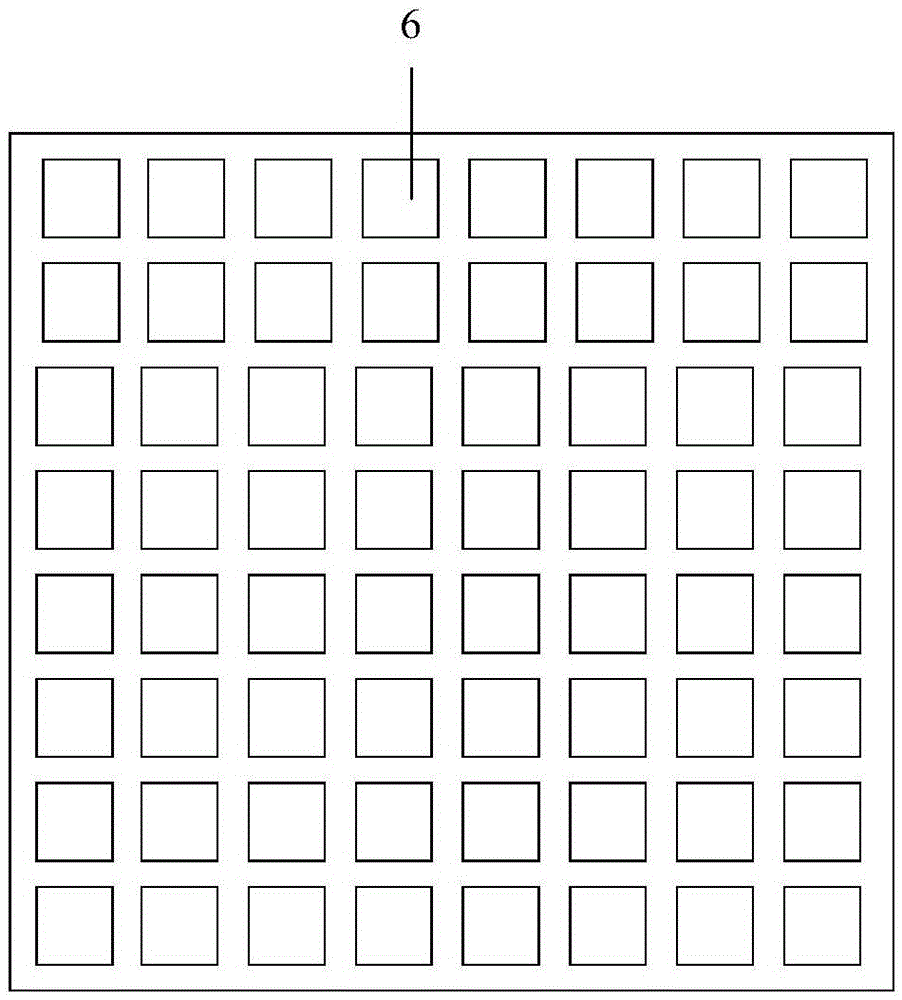
[0059] A polyimide tape is selected as the mask 1. The mask 1 has hollowed-out cells arranged in a matrix of six rows and six rows. Each cell is separated by a non-conductive mask 1 and has a distance of 3mm. The length and width of each hollowed-out unit cell are 1×1mm, and the above-mentioned mask 1 is covered on the surface of the ...

Embodiment 3

[0075] The glass substrate whose surface is deposited with indium oxide tin-doped thin film (lower transparent conductive layer) is fixed on the sample holder in the vacuum chamber of magnetron sputtering instrument; Wherein, the glass substrate with surface deposited with indium oxide tin-doped thin film can be directly outside You can also choose indium oxide-doped tin target material, and use magnetron sputtering to plate on the surface of the glass substrate. In this embodiment, for the convenience of the experiment, the glass substrate with the indium oxide-doped tin film on the surface is used as the first substrate ;

[0076] A polyimide tape is selected as the mask 1, the mask 1 has hollow cells arranged in a matrix of three rows and five rows, and each cell is separated by a non-conductive mask 1 with a distance of 3 mm. The length and width of each hollowed-out cell are 2×2mm, and the above-mentioned mask 1 is covered on the surface of the above-mentioned first substra...


PUM

PropertyMeasurementUnit
thermal resistanceaaaaaaaaaa
thicknessaaaaaaaaaa
thicknessaaaaaaaaaa

Abstract

The invention discloses an electrochromic device for screening solid inorganic electrochromic materials at high throughput and a manufacturing method of the electrochromic device. The problem that optimal electrochromic materials cannot be accurately screened out is solved. The electrochromic device comprises a substrate, a lower transparent conducting layer and multiple electrochromic device units on the lower transparent conducting layer. The units are divided into at least two groups, and each unit is provided with a cathode electrochromic layer, a solid electrolyte layer, an anode electrochromic layer and an upper transparent conducting layer from inside to outside. A thickness gradually-changing layer is formed on at least one functional layer of the cathode electrochromic layers, the solid electrolyte layers and the anode electrochromic layers. When the functional layers are made of one material, the thicknesses of the same functional layers in the units in different groups are different, and the thickness gradually-changing layers are formed. When the functional layers are made of two or more materials, the thickness ratios of the same functional layers in the units in different groups are different, and composite thickness gradually-changing layers are formed. The electrochromic device is used for the high throughput technology and can accurately screen out the optimal electrochromic materials.

Description

technical field [0001] The invention relates to the field of electrochromic materials, in particular to an electrochromic device for high-throughput screening of solid inorganic electrochromic materials and a preparation method thereof. Background technique [0002] Electrochromism refers to the phenomenon that the optical properties of materials (reflectivity, light transmittance and absorptivity, etc.) undergo a stable and reversible color change under the action of an external electric field, which is manifested as a reversible change in color and transparency in appearance. Materials with electrochromic properties are called electrochromic materials; devices made of electrochromic materials are called electrochromic devices. The working principle of electrochromism is that the electrochromic material undergoes an electrochemical redox reaction under the action of an external electric field, gaining and losing electrons, and changing the color of the material. Electrochr...

Claims


Application Information

Patent Timeline
Patent Type & Authority Applications(China)
IPC IPC(8): G02F1/153G02F1/155
CPCG02F1/153G02F1/155G02F2001/15145
Inventor 孟政闫宁宁刘静汪洪
Owner CHINA BUILDING MATERIALS ACAD
Why Eureka
Try Eureka