Single photon imaging detector and manufacturing method thereof

A technology of imaging detector and manufacturing method, applied in radiation control devices and other directions, can solve problems such as poor coupling, and achieve the effects of low power consumption, low cost, and no cooling required

Inactive Publication Date: 2016-05-25
INST OF MICROELECTRONICS CHINESE ACAD OF SCI
View PDF8 Cites 11 Cited by
  • Summary
  • Abstract
  • Description
  • Claims
  • Application Information

AI Technical Summary

Problems solved by technology

The imaging detection device formed by direct coupling with a charge-coupled device (CCD, Charge-coupled Device) or a complementary metal oxide semiconductor (CMOS, ComplementaryMetalOxideSemiconductor) has the disadvantage of poor coupling

Method used


Image

  • Single photon imaging detector and manufacturing method thereof
  • Single photon imaging detector and manufacturing method thereof
  • Single photon imaging detector and manufacturing method thereof

Examples


Embodiment 1

[0042] This embodiment provides a method for manufacturing a single-photon imaging detector, including the following steps:

[0043]Step 110, preparing a silicon-based microchannel plate, the silicon-based microchannel plate is provided with an array of micro-through holes;

[0044] Specifically, a silicon wafer is used as the substrate, and a microhole array is formed on the substrate by silicon micro-via etching forming technology, and then a microchannel inner wall functional layer is prepared on the microhole array by chemical vapor deposition, forming Silicon-based microchannel plate; the above steps can ensure the high precision of the micropore size, and the size of the silicon-based microchannel plate can achieve a larger area, which is convenient for mass production;

[0045] Step 120, preparing CMOS imaging sensor array

[0046] Specifically, the step 120 includes the following steps:

[0047] Step 1201, forming a gradient-doped PinnedPhotodiode structure on the su...

Embodiment 2

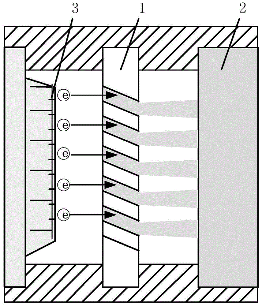
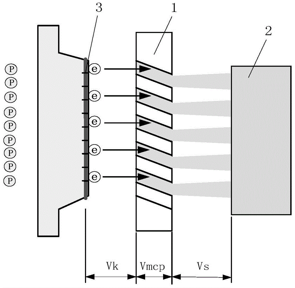
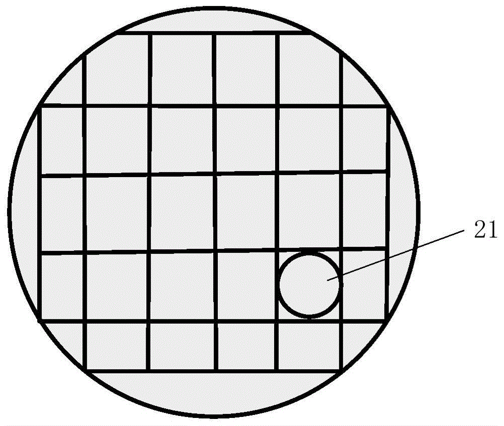
[0070] Such as figure 1 As shown, the present embodiment provides a fast single-photon imaging detector, obtained by the manufacturing method of Embodiment 1, comprising a silicon-based microchannel plate 1, a CMOS imaging sensor array 2 and a photocathode 3, the silicon-based microchannel plate 1 is provided with a micro-via array, and the CMOS imaging sensor array 2 is an array of several imaging sensors 21 arranged on a silicon substrate, and the photocathode 3 is translucent; when light irradiates the translucent photoelectric On the cathode, the electric field between the photocathode 3 and the silicon-based microchannel plate 1 pushes the electrons released from the surface of the photocathode 3 into the silicon-based microchannel plate 1, and the silicon-based microchannel plate 1 will to 10 4 -10 8 The number of electrons is amplified by an order of magnitude, and the magnification is controlled by adjusting the amplification voltage at both ends of the silicon-based...


PUM


Abstract

The invention relates to the technical field of photoelectric imaging detection, and particularly relates to a single photon imaging detector and a manufacturing method thereof. The manufacturing method comprises the following steps: a silicon substrate microchannel plate is manufactured, and a micro through hole array is arranged in the silicon substrate microchannel plate; a CMOS (Complementary Metal Oxide Semiconductor) imaging sensor array is manufactured; a photoelectric cathode is manufactured and tested in a packaging device, device wafer level structural integration is carried out on the silicon substrate microchannel plate, the CMOS imaging sensor array and the photoelectric cathode, the single photon imaging detector is formed, and the single photon imaging detector is tested. The wafer level packaging processing technology is adopted, the photoelectric cathode, the silicon substrate microchannel plate and the CMOS imaging sensor array are directly coupled, and a high-flexibility, high-speed, high-resolution, low-cost, low-power consumption, high-frame frequency, no-cooling and compact-size single photon imaging detector.

Description

technical field [0001] The invention relates to the technical field of photoelectric imaging detection, in particular to a single-photon imaging detector and a manufacturing method thereof. Background technique [0002] With the development of biomedicine, space detection and environmental radiation detection technology, the detection requirements for weak light are getting higher and higher, and because of the extremely weak target, it is impossible to use traditional cameras and conventional detection technology to obtain images, especially when the light is too weak When a single photon is emitted, general low-light imaging devices cannot meet the demand. Therefore, single-photon imaging detection technology has become a research hotspot in the current international scientific and technological circles. Traditional imaging devices based on Charge-Coupled Device (CCD, Charge-coupled Device) and Complementary Metal Oxide Semiconductor (CMOS, Complementary Metal Oxide Semico...

Claims


Application Information

Patent Timeline
Patent Type & Authority Applications(China)
IPC IPC(8): H01L27/146
Inventor 李成敏严冬刘健鹏刘涛
Owner INST OF MICROELECTRONICS CHINESE ACAD OF SCI
Why Eureka
Try Eureka