Thin film transistor and manufacturing method, array substrate and display device

A technology for thin film transistors and a manufacturing method, applied in the field of display processing, can solve the problems of under-etching or over-etching of contact holes, adverse effects of thin-film transistors, and difficulty in mastering the etching process, so as to prevent etching to the active layer and prevent over-etching. The effect of engraving and improving yield

Inactive Publication Date: 2016-05-25
BOE TECH GRP CO LTD
View PDF4 Cites 5 Cited by
  • Summary
  • Abstract
  • Description
  • Claims
  • Application Information

AI Technical Summary

Problems solved by technology

[0005] At present, when etching a contact hole on an insulating layer, due to the difficulty in mastering the etching process, the contact hole is often under-etched or over-etched, which will have a negative impact on the thin film transistor and reduce the yield of the thin film transistor.

Method used


Image

  • Thin film transistor and manufacturing method, array substrate and display device
  • Thin film transistor and manufacturing method, array substrate and display device
  • Thin film transistor and manufacturing method, array substrate and display device

Examples


Embodiment 1

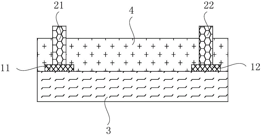
[0054] An embodiment of the present invention provides a thin film transistor, see Figure 1-Figure 6 , the thin film transistor includes:

[0055] The first etching barrier layer 11, the second etching barrier layer 12, the source electrode 21, the drain electrode 22, the insulating layer 4 and the active layer 3;

[0056] The first etch barrier layer 11 and the second etch barrier layer 12 are disposed on the active layer 3, the insulating layer 4 is disposed on the active layer 3, the first etch barrier layer 11 and the second etch barrier layer 12, The insulating layer 4 is provided with a first contact hole 51 and a second contact hole 52;

[0057] The source electrode 21 is electrically connected to the active layer 3 through the first contact hole 51, and the drain electrode 22 is electrically connected to the active layer 3 through the second contact hole 52;

[0058] The first etch stop layer 11 is located between the active layer 3 and the source 21 , and the secon...

Embodiment 2

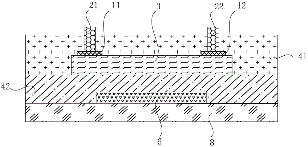
[0089] On the other hand, the embodiment of the present invention further provides an array substrate, and the array substrate includes the thin film transistor described in the first embodiment.

[0090] The array substrate provided in this embodiment includes the thin film transistor described in Embodiment 1. The thin film transistor in Embodiment 1 solves the problem of under-etching or over-etching in the contact hole etching process, and improves the yield of thin film transistors. At the same time, the first embodiment The material of the first etch barrier layer 11 is the same as the material of the first layer in the source electrode 21, and the first etch barrier layer 11 is connected to the material of the first layer in the source electrode 21, and the material of the first etch barrier layer 11 is the same as that of the first layer of the source electrode 21. The material of the second etch barrier layer 12 is the same, and the structure and material of the source...

Embodiment 3

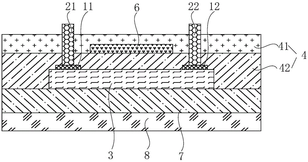
[0092] On the other hand, the embodiment of the present invention further provides a display device, the display device includes the array substrate described in the second embodiment.

[0093] The display device provided in this embodiment includes the array substrate of the second embodiment. The array substrate of the second embodiment solves the problem of under-etching or over-etching in the contact hole etching process, and improves the yield of the array substrate. At the same time, the first engraving The material of the etch barrier layer 11 is the same as that of the first layer in the source electrode 21, and the first etch barrier layer 11 is connected with the material of the first layer in the source electrode 21, and the material of the first etch barrier layer 11 is the same as that of the second layer. The material of the etch barrier layer 12 is the same, and the structure and material of the source electrode 21 and the drain electrode 22 are all the same, so ...


PUM


Abstract

The invention discloses a thin film transistor and a manufacturing method, an array substrate and a display device, and belongs to the field of display processing technology. The thin film transistor comprises a first etching barrier layer, a second etching barrier layer, a source, a drain, an insulating layer and an active layer; the insulating layer is arranged on the active layer, the first etching barrier layer and the second etching barrier layer, and the insulating layer is provided with a first contact hole and a second contact hole; the source is electrically connected with the active layer via the first contact hole, and the drain is electrically connected with the active layer via the second contact hole; the first etching barrier layer is positioned between the active layer and the source; and the second etching barrier layer is positioned between the active layer and the drain. When the insulating layer is etched with the contact holes, the contact holes can be directly etched onto the first etching barrier layer and the second etching barrier layer to prevent under-etching, and the first etching barrier layer and the second etching barrier layer block the active layer to prevent the active layer from being etched and prevent over-etching, so that the yield of the thin film transistor is improved.

Description

technical field [0001] The invention relates to the field of display processing, in particular to a thin film transistor, a manufacturing method, an array substrate, and a display device. Background technique [0002] Thin-film transistors are used to make displays with high-end display effects. The light emitted by each pixel on the display is driven by an integrated thin-film transistor behind it. [0003] At present, the manufacturing method of a thin film transistor includes: forming an active layer, the active layer includes a source doped region and a drain doped region, depositing an insulating layer on the active layer, respectively insulating the doped source region layer and the insulating layer above the doped drain region are etched to expose the doped source region and the doped drain region and form two contact holes, and a source and drain metal layer is deposited on the insulating layer, which is formed after the patterning process source and drain. [000...

Claims


Application Information

Patent Timeline
Patent Type & Authority Applications(China)
IPC IPC(8): H01L29/786H01L27/12
CPCH01L27/1214H01L29/786H01L29/66757H01L29/66765H01L27/1248H01L29/458H01L29/41733H01L29/78675H01L29/78678H10K59/12H01L21/76832H01L27/1218H01L29/6675H01L29/78663
Inventor 张慧娟刘建宏
Owner BOE TECH GRP CO LTD
Why Eureka
Try Eureka