Highly Selective and Angularly Stable Frequency Selective Surfaces
A frequency-selective surface and selectivity technology, which is applied in the microwave field, can solve the problems that selectivity and angle stability cannot be taken into account at the same time, and achieve the effects of simple structure, improved Q value, and improved selectivity
- Summary
- Abstract
- Description
- Claims
- Application Information
AI Technical Summary
Problems solved by technology
Method used
Image
Examples
Embodiment 1
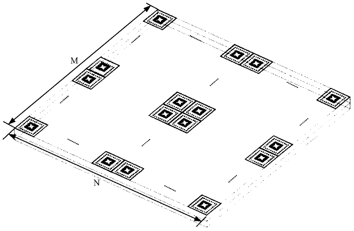
[0028] refer to figure 1 , the present invention is formed by periodic arrangement of M×N passive resonant units, wherein M≥3, N≥3.
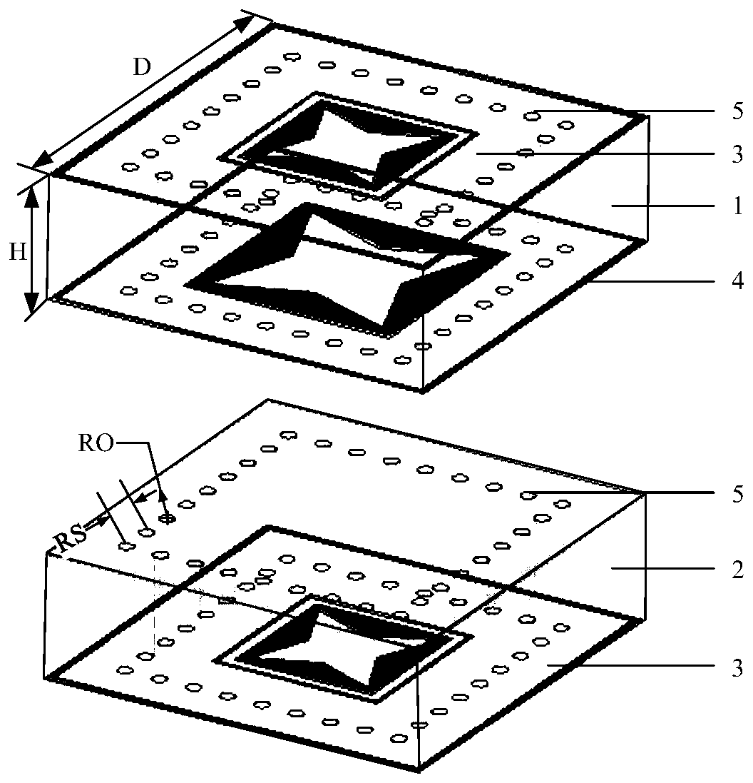
[0029] refer to figure 2 , the passive resonant unit includes a first dielectric substrate 1, a second dielectric substrate 2, a first radiation patch 3, a second radiation patch 4, and a dielectric through hole 5; wherein the first dielectric substrate 1 and the second dielectric substrate 2 are up and down Form a stacked structure, through the stacked structure of two dielectric substrates, the Q value of the formed frequency selective surface equivalent circuit can be improved, so as to improve the selectivity of the frequency selective surface; the first dielectric substrate 1 and the second dielectric substrate 2 Both are provided with a plurality of dielectric through holes 5 penetrating up and down to improve the selectivity of the formed frequency selective surface structure; these dielectric through holes 5 are arranged in a square, a...
Embodiment 2
[0033] The structure of this embodiment is the same as that of Embodiment 1, and only the following parameters are adjusted:
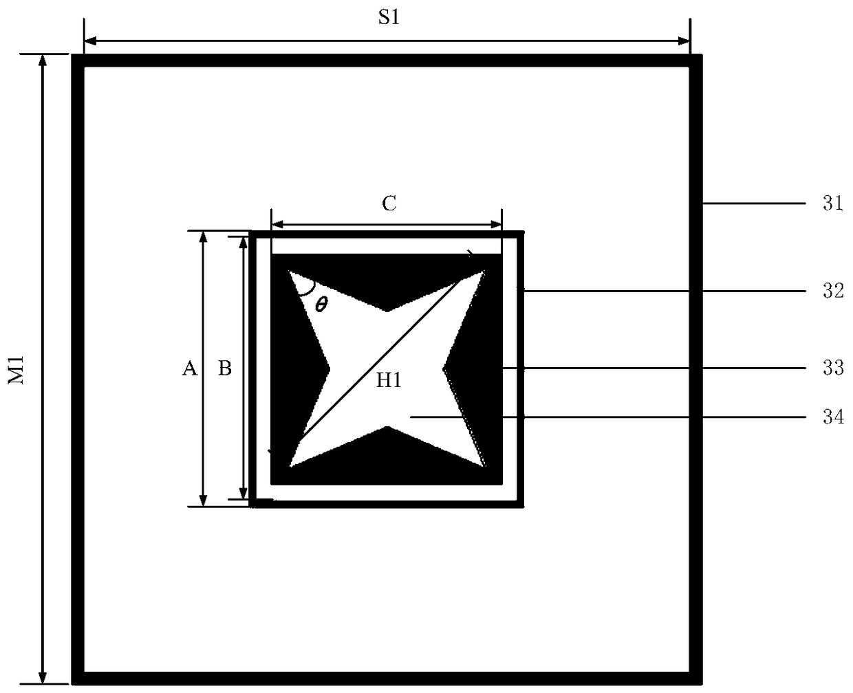
[0034] The side length D of the first dielectric substrate 1 and the second dielectric substrate 2 = 5.4 mm, the thickness H = 1.5 mm; the radius RO of the dielectric through hole 5 = 0.1 mm; the distance RS between the centers of adjacent dielectric through holes = 0.5 mm; The outer side length M1=5.4mm of one side ring 31, the inner side length S1=5.3mm; the outer side length A=2.4mm of the second side ring 32, the inner side length B=2.3mm; the side of the first square patch 33 Long C=1.8mm, the diagonal length H1=2.5mm of the first regular four-pointed star gap 34, angle θ=40 °; The outer length M2=5.5mm of the third party ring 41, the inner length S2=5.4mm; The side length P=2.8mm of the two square patches 42, the diagonal length H2=3.4mm of the second positive four-pointed star gap 43, the angle
Embodiment 3
[0036] The structure of this embodiment is the same as that of Embodiment 1, and only the following parameters are adjusted:
[0037] The dimensions of the first dielectric substrate 1 and the second dielectric substrate 2 are D=5.7mm, H=2mm, the radius RO of the dielectric through hole 5=0.2mm, the distance between the centers of adjacent dielectric through holes RS=0.7mm, and the first square ring The outer side length M1 of 31=5.7mm, the inner side length S1=5.4mm, the outer side length A=2.6mm of the second square ring 32, the inner side length B=2.1mm, the side length C=2mm of the first square patch , the diagonal length H1=2.3mm of the first square star gap 34, the angle θ=45°, the outer side length M2=5.7mm of the third party ring 41, and the inner side length S2=5.4mm; the second square patch Side length P=3.1mm, the diagonal length H2=3.7mm of the second regular four-pointed star gap 43, angle
[0038] The technical effect of the present invention is further descri...
PUM
 Abstract
Description
Claims
Application Information


