Device for transition from rectangular waveguide to substrate integrated waveguide on Ka-band

A substrate-integrated waveguide and rectangular waveguide technology, which is applied in connection devices, waveguide devices, electrical components, etc., can solve the problems of large insertion loss, large circuit size, and difficult processing, and achieve low insertion loss and miniaturized insertion loss , the effect of simple structure

Inactive Publication Date: 2016-05-25
UNIV OF ELECTRONIC SCI & TECH OF CHINA
View PDF4 Cites 17 Cited by
  • Summary
  • Abstract
  • Description
  • Claims
  • Application Information

AI Technical Summary

Problems solved by technology

These transition structures are difficult to meet the volume, bandwidth, insertion loss and other requirements at the same time. For example, the tapered fin-line transition structure has a large circuit size, and the ridge-shaped stepped waveguide transition structure has a large insertion loss and is not easy to process.

Method used


Image

  • Device for transition from rectangular waveguide to substrate integrated waveguide on Ka-band
  • Device for transition from rectangular waveguide to substrate integrated waveguide on Ka-band
  • Device for transition from rectangular waveguide to substrate integrated waveguide on Ka-band

Examples


Embodiment Construction

[0022] The present invention will be further described below in conjunction with accompanying drawing and specific embodiment:

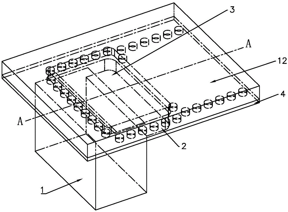
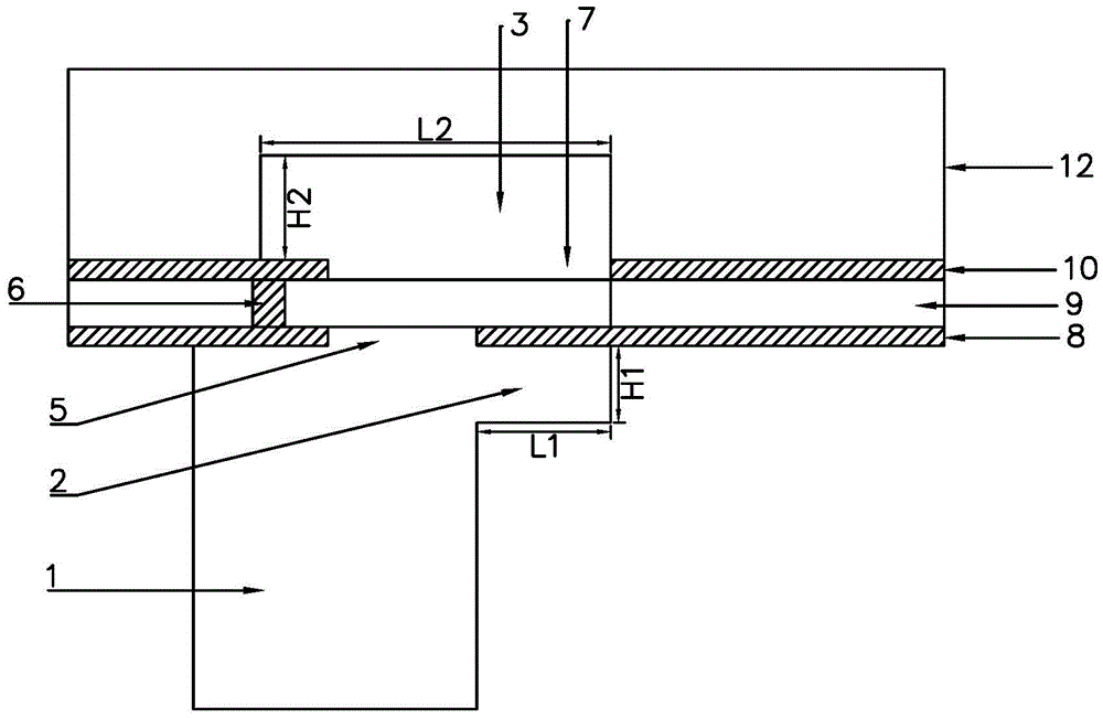
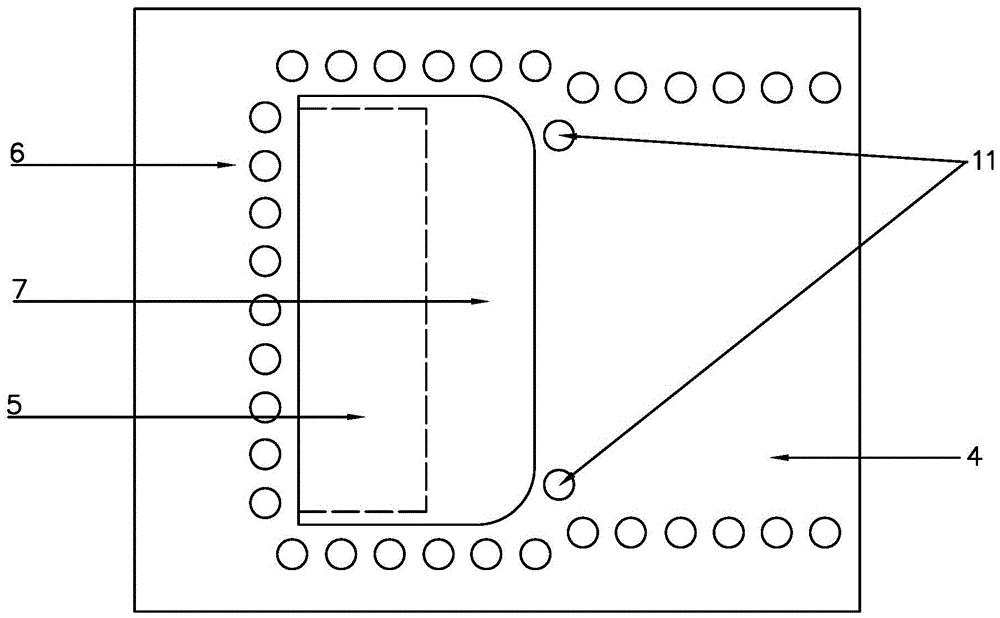
[0023] like Figure 1-3 As shown, the device for converting a Ka-band rectangular waveguide to a substrate-integrated waveguide of the present invention includes a rectangular waveguide 1, a substrate-integrated waveguide 4, and an upper metal plate 12 with a rectangular groove on the bottom surface arranged in sequence from bottom to top. The substrate integrated waveguide 4 includes a lower metal 8 , a dielectric substrate 9 and an upper metal 10 , and the dielectric substrate 9 is provided with a metallized via hole array 6 connecting the upper metal 10 and the lower metal 8 . The upper part of the broad side of the rectangular waveguide 1 protrudes outwards and the cavity formed with the lower metal sheet 8 is the first resonant cavity 2 . The cavity two formed by the rectangular groove and the upper metal sheet 12 is the second resonant cavity ...


PUM

PropertyMeasurementUnit
Center distanceaaaaaaaaaa

Abstract

The invention discloses a device for transition from a rectangular waveguide to a substrate integrated waveguide on a Ka-band. The device comprises the rectangular waveguide, a first resonant cavity, the substrate integrated waveguide and a second resonant cavity, which are sequentially arranged from bottom to top, wherein the substrate integrated waveguide comprises a dielectric substrate, an upper metal sheet and a lower metal sheet; the upper metal sheet and the lower metal sheet are arranged on the upper surface and the lower surface of the dielectric substrate; a first coupling window is formed in the position, corresponding to a rectangular waveguide opening, of the lower metal sheet; and a second coupling window is formed in the position, corresponding to the second resonant cavity, of the upper metal sheet. The device has the advantages of small volume, small insertion loss and large bandwidth, and is suitable for application of right-angle transition of the Ka-band broadband, simple in structure, easy to fabricate and worthy of industry promotion; and mass production is achieved.

Description

technical field [0001] The invention belongs to the technical field of microwave and millimeter wave integration, and in particular relates to a device for converting a Ka-band rectangular waveguide into a substrate integrated waveguide. Background technique [0002] Substrate Integrated Waveguide (Substrate Integrated Waveguide) is a new type of waveguide structure proposed in recent years. It is composed of two rows of metallized through holes on the left and right, two layers of metal surfaces on the upper and lower sides, and a low-loss dielectric layer filled in the middle. Transmission properties of waveguides. It has the advantages of low loss, high Q value, low cost, and easy integration, which solves the problem that traditional metal waveguides are difficult to integrate and miniaturize. Since the entire structure is completely composed of metal via arrays on the dielectric substrate, multi-layer printing can be used Circuit board (PCB) or low temperature co-fired...

Claims


Application Information

Patent Timeline
IPC IPC(8): H01P5/08
CPCH01P5/08
Inventor 夏雷郎小元徐锐敏延波
Owner UNIV OF ELECTRONIC SCI & TECH OF CHINA
Why Eureka
Try Eureka