Printed circuit board

A technology of printed circuit boards and contact circuits, which is applied in the direction of printed circuits, printed circuit manufacturing, printed circuit components, etc., can solve the problems of slow production and processing speed, inconvenient maintenance and disassembly, and multiple PCB wiring areas, so as to reduce production costs , The effect of reducing maintenance costs

Inactive Publication Date: 2016-05-25
AKM ELECTRONICS TECH SUZHOU
View PDF5 Cites 3 Cited by
  • Summary
  • Abstract
  • Description
  • Claims
  • Application Information

AI Technical Summary

Problems solved by technology

For wire connection, the process is difficult, the production and processing speed is slow, it is not suitable for mass production, and the existence of connecting wires will occupy a large amount of circuit space, and it is not convenient for later maintenance and disassembly
For the shrapnel connector connection, specifically, it uses the shrapnel connector to connect two superimposed circuit boards. Although this method can meet the requirements of rapid production and processing, the disadvantages are also obvious: ①The addition of the connector takes up More PCB wiring area and increase the thickness of the circuit board, which is not conducive to the thin and light design of the product; ②The price of the connector is usually relatively expensive, which increases the manufacturing cost of electronic products

Method used


Image

  • Printed circuit board
  • Printed circuit board

Examples


Embodiment 1

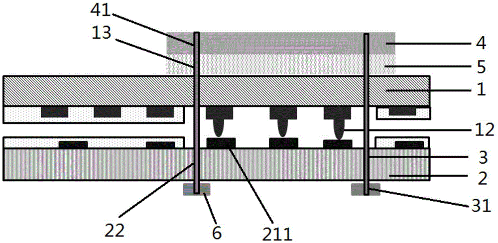
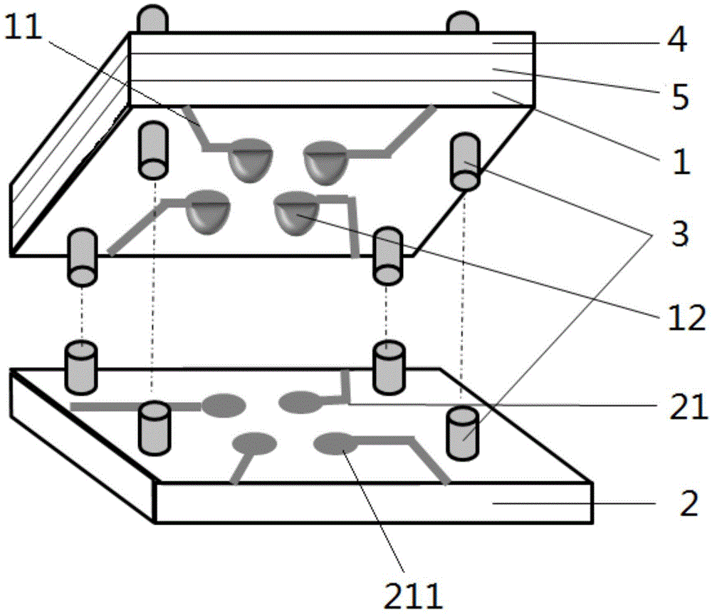
[0026] This embodiment discloses a printed circuit board, refer to Figure 1~2 , including an FPC daughter board 1 and a PCB mother board 2, the FPC daughter board 1 is installed on the PCB mother board 2, the FPC daughter board 1 is provided with a conductive convex hull 12, and the PCB motherboard 2 is provided with a conductive convex hull 12 Corresponding to the contact circuit 211 , the conductive protrusion 12 is in contact with the corresponding contact circuit 211 , so as to realize the circuit connection between the FPC sub-board 1 and the PCB motherboard 2 . For the printed circuit board disclosed in this embodiment, a more specific description is as follows:

[0027] like Figure 1~2 As shown, a first connection line 11 (including components) is laid on the FPC sub-board 1 , wherein the first connection line 11 is laid by a conventional process, and the components are laid by a conventional welding method. After the laying of the first connection line 11 and the s...


PUM


Abstract

The invention discloses a printed circuit board (PCB). The printed circuit board comprises a PCB mother board and is characterized in that a flexible printed circuit (FPC) daughter board is arranged on the PCB mother board, the FPC daughter board and the PCB mother board are in contact with corresponding contact circuits through conductive bulges so that a conductive path is formed between the FPC daughter board and the PCB mother board, a hard thin sheet is fixedly arranged on the back surface of the side where the conductive bulges are located, the protruding heights of the conductive bulges are 30-300 micrometers, and the diameters of the conductive bulges are phi 50-800 micrometers. In the PCB, the FPC daughter board and the PCB mother board can be conveniently and rapidly disassembled repeatedly, the PCB is suitable for mass production, and the production cost and the subsequent maintenance cost are favorably reduced; and moreover, the wiring area of the PCB can be fully utilized, the light and thin design is promoted, and the PCB conforms to a scientific trend.

Description

technical field [0001] The invention belongs to the technical field of printed circuit boards (PCBs), and in particular relates to a printed circuit board. Background technique [0002] In modern society, the information industry is developing rapidly, and electronic products are showing a trend of thinning, miniaturization, and multi-function. Printed circuit board (PCB) is an important electronic component in electronic products. It is not only an electronic component The supporting body of the device is also the provider of the electrical connection of the electronic components. Therefore, the packaging area of ​​the PCB has become a key point that must be considered in the design and manufacture of electronic products. [0003] In the mounting production of PCB surface devices, the copper clad layer on the surface of the PCB is generally used to arrange lines and components. In this process, the space utilization rate of the PCB is low, and the number of functional devic...

Claims


Application Information

Patent Timeline
Patent Type & Authority Applications(China)
IPC IPC(8): H05K1/14
CPCH05K1/141H05K3/365
Inventor 孙彬崔成强张仕通
Owner AKM ELECTRONICS TECH SUZHOU
Why Eureka
Try Eureka