

Level offset unit, level offset circuit and drive method, and grid drive circuit
A technology of level shifting and driving power, applied in electrical components, logic circuits, logic circuit interface devices, etc., can solve problems such as safety hazards, scrapped display devices, and gate driver current burning, and achieve the effect of avoiding burning
- Summary
- Abstract
- Description
- Claims
- Application Information
AI Technical Summary
Problems solved by technology
Method used
Image

Examples
Embodiment 1
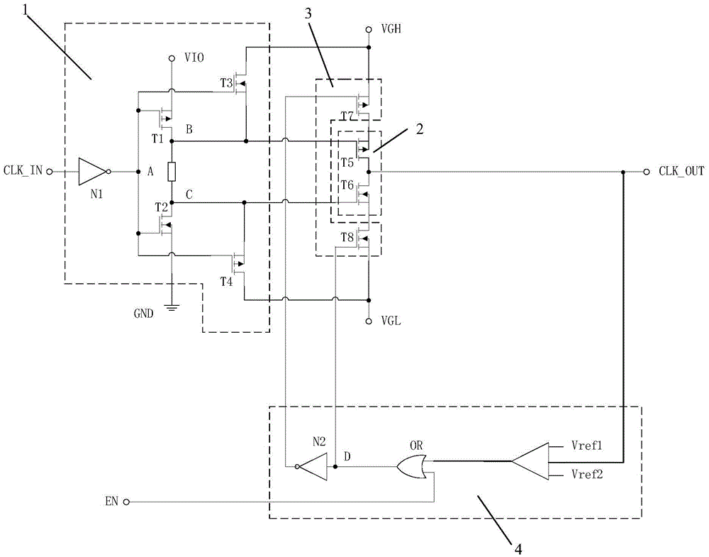
[0049] to combine figure 1 As shown, this embodiment provides a level shift unit, including: a logic control module 1, an output module 2, an output control module 3, and a feedback module 4; wherein, the logic control module 1 is connected to a power supply, a drive power , the input signal terminal CLK_IN, and the output module 2, which are used to generate a control signal opposite to the input signal, and select the logic level signal input by the drive power supply corresponding to the polarity of the power supply according to the control signal, and convert the The logic level signal is transmitted to the output module 2; the feedback module 4 is connected to the enable signal terminal EN, the signal output terminal CLK_OUT, and the output control module 3, for according to the enable signal terminal EN and the The signal input by the signal output terminal CLK_OUT outputs a feedback signal and transmits it to the output control module 3; the output control module 3 is c...
Embodiment 2
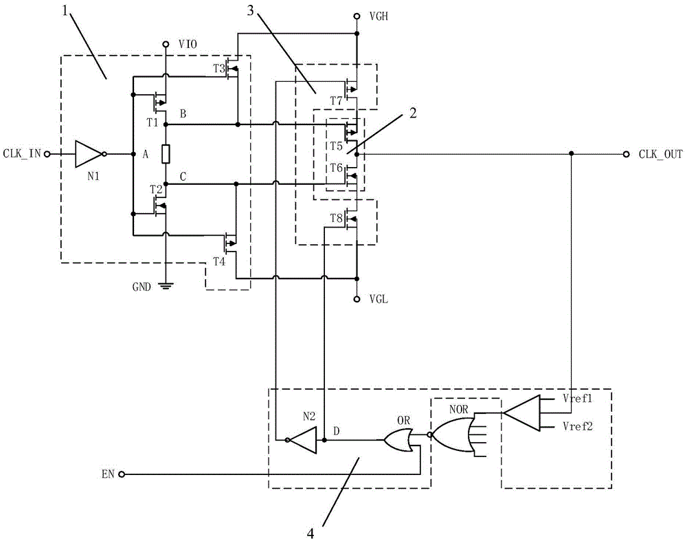
[0067] Such as figure 1 and 3 As shown, this embodiment provides a level shifting circuit, which includes a plurality of level shifting units described in Embodiment 1.
[0068] Wherein, when the feedback module 4 includes a voltage comparator, an OR gate OR and a second inverter N2, the preferred level shifting circuit in this embodiment also includes a NOR gate NOR; wherein, the NOR gate NOR One input terminal is connected to the output terminal of a voltage comparator of the feedback module 4 , and the output terminal is connected to the first input terminal of the OR gate OR of each feedback module 4 .
[0069] Specifically, the enable signal terminal EN inputs a high-level signal at power-on, and the enable signal terminal EN inputs a low-level signal at other times. In this implementation, at the time of power-on, one input terminal (second input terminal) of the OR gate OR inputs a high level enable signal, and the other input terminal (first input terminal) no matter...
Embodiment 3
[0072] This embodiment provides a method for driving a level shift circuit, wherein the level shift circuit includes the level shift unit in Embodiment 1 of multiple embodiments. The driving method specifically includes the following steps.
[0073] refer to figure 1 and 4 As shown, the power-on output stage: If the signal VIO=3.3V input by the working voltage terminal VIO of the power supply is turned on, the working ground terminal is grounded; the signal VGH=30V input by the high-level signal terminal VGH of the drive power supply, low-level The signal VGL input by the signal terminal VGL=-8V.
[0074] At the time of power-on, the enable signal terminal EN inputs a high-level signal, and the enable signal terminal EN inputs a low-level signal at other times. Therefore, when the power is turned on, one input of the OR gate OR inputs a high-level enable signal, and the other port no matter whether the input is high-level or low-level, at this time the output of the OR gate...
PUM
 Abstract
Description
Claims
Application Information