Removing method of native oxide layer of FinFet device before source-drain epitaxy

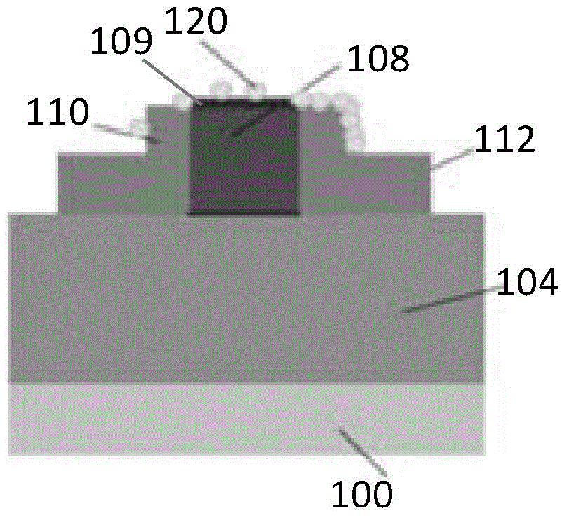
A natural oxide layer, source-drain technology, applied in semiconductor/solid-state device manufacturing, electrical components, circuits, etc., can solve the problems of sidewall 110 and mask layer 109 loss, device failure, etc., to avoid mushroom "defects, The effect of reducing loss and good process control

Inactive Publication Date: 2016-06-01
INST OF MICROELECTRONICS CHINESE ACAD OF SCI
View PDF6 Cites 0 Cited by
  • Summary
  • Abstract
  • Description
  • Claims
  • Application Information

AI Technical Summary

Problems solved by technology

In the HF-last process, the natural oxide layer is usually completely removed by controlling the etching time, but the problem is that if the rinsing time is too long, too much loss of the sidewall 110 and the mask layer 109 will be caused, making the false gate The gate 108 exposes a defect that would form a "mushroom" 109 during the selective epitaxial process, see image 3 As shown, connecting the source and drain will cause the failure of the device

Method used


Image

  • Removing method of native oxide layer of FinFet device before source-drain epitaxy
  • Removing method of native oxide layer of FinFet device before source-drain epitaxy
  • Removing method of native oxide layer of FinFet device before source-drain epitaxy

Examples


Embodiment Construction

[0022] In order to make the above objects, features and advantages of the invention more obvious and comprehensible, specific implementations of the invention will be described in detail below.

[0023] In the following description, a lot of specific details are set forth in order to fully understand the present invention, but the present invention can also be implemented in other ways different from those described here, and those skilled in the art can do it without departing from the meaning of the present invention. By analogy, the present invention is therefore not limited to the specific examples disclosed below.

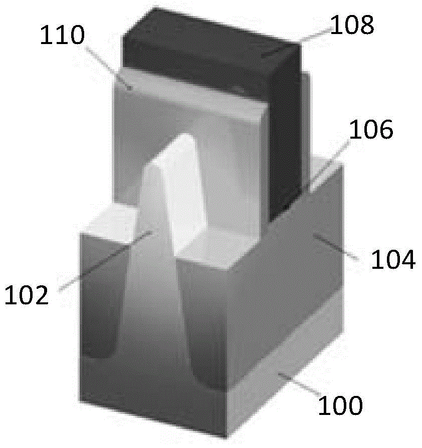
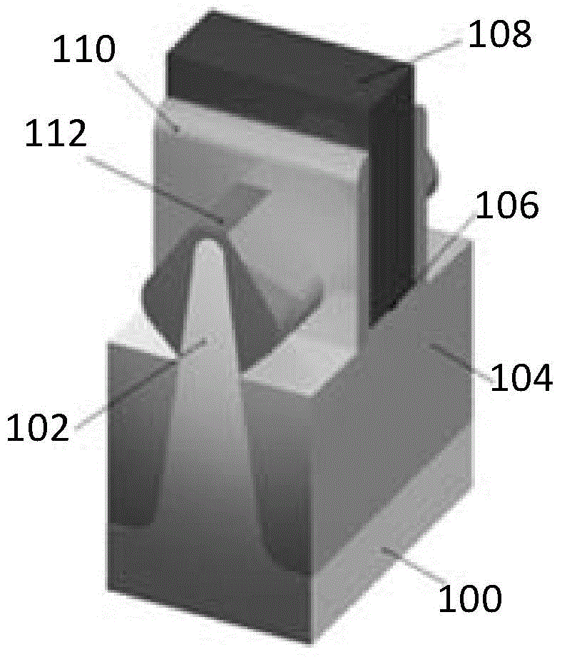
[0024] The present invention provides a method for removing the natural oxide layer before the source-drain epitaxy of a FinFET device, that is, before the source-drain epitaxy process is required, the natural oxide layer on the surface of the exposed fin is removed. Usually, in this step wherein the device includes: fins; isolation between the fins; gates on ...


PUM


Abstract

The invention provides a removing method of a native oxide layer of a FinFet device before source-drain epitaxy. The method comprises the steps: performing RCA cleaning, and removing the native oxide layer in a waterless HF gas phase corrosion. The method has good process control performance, and contact between oxygen and a surface of a wafer can be cut off well. The native oxide layer is effectively removed, loss of other area medium layers is reduced at the same time, and a mushroom defect in a subsequent selectivity epitaxial process is prevented from generation.

Description

technical field [0001] The invention relates to the field of semiconductor device preparation, in particular to a method for removing a natural oxide layer before source and drain epitaxy of a FinFet device. Background technique [0002] Fin-FET is a transistor with a fin-type channel structure, which uses several surfaces of a thin fin as a channel, thereby preventing the short-channel effect in conventional transistors and increasing the operating current at the same time. [0003] At present, in the FinFet device manufacturing process, in order to increase the carrier mobility to meet the device speed requirements, different materials are usually introduced into the source and drain regions of NMOS and PMOS transistors to introduce pressure into the channel. The usual practice is that for PMOS devices, a stress layer of SiGe is epitaxially grown on the source and drain regions of the fin. Since the lattice constant of SiGe is larger than that of Si, the stress layer will ...

Claims


Application Information

Patent Timeline
Patent Type & Authority Applications(China)
IPC IPC(8): H01L21/311
Inventor 王桂磊崔虎山殷华湘李俊峰赵超
Owner INST OF MICROELECTRONICS CHINESE ACAD OF SCI
Why Eureka
Try Eureka