non-volatile memory

A non-volatile, memory technology, used in semiconductor devices, electro-solid devices, electrical components, etc., can solve the problems of low turn-on current, poor maintenance performance, affecting transistor performance, etc., to reduce charge loss and improve maintenance performance.

Active Publication Date: 2019-05-24
EMEMORY TECH INC
View PDF3 Cites 0 Cited by
  • Summary
  • Abstract
  • Description
  • Claims
  • Application Information

AI Technical Summary

Problems solved by technology

The contact etch stop layer is made of silicon nitride formed by plasma-enhanced chemical vapor deposition, which will cause the floating gate transistor to have low on-current (Low On Current) and poor retention performance.
However, if the material of the contact etch stop layer is changed, the performance of the transistors in the peripheral circuit area will be affected.

Method used


Image

  • non-volatile memory
  • non-volatile memory
  • non-volatile memory

Examples


Embodiment Construction

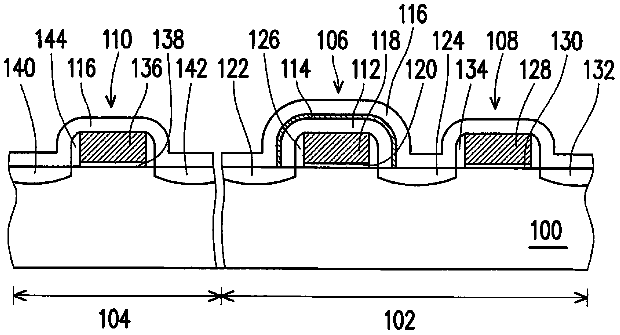
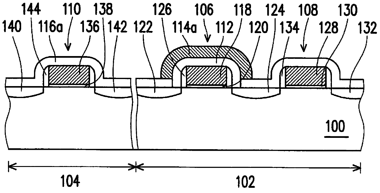
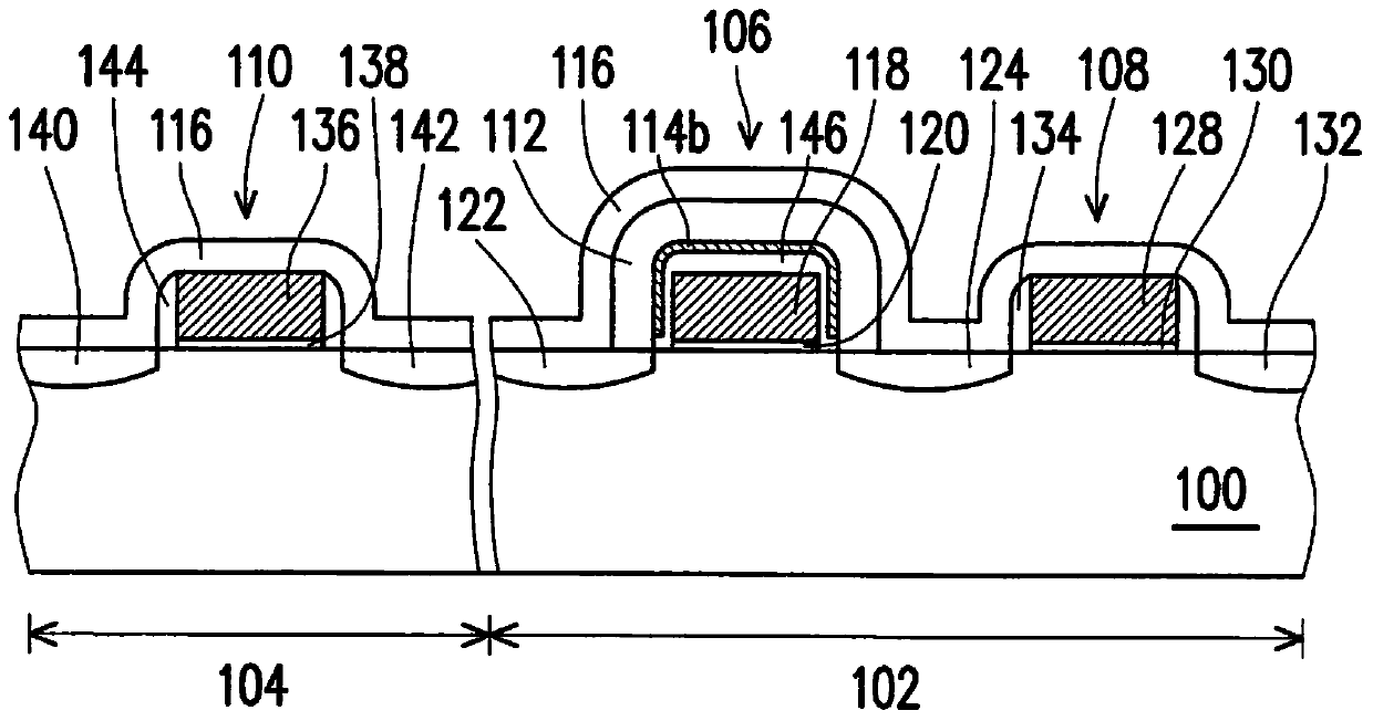
[0046] figure 1 It is a sectional view of a non-volatile memory in a preferred embodiment of the present invention. Please refer to figure 1 , the non-volatile memory of the present invention is disposed on the substrate 100 . The substrate 100 is, for example, a silicon substrate. The substrate 100 has a memory cell area 102 and a peripheral circuit area 104 .

[0047] The non-volatile memory includes a floating gate transistor 106 , a select gate transistor 108 , a transistor 110 , a self-aligned barrier layer 112 , a tensile layer 114 , and a contact etch stop layer 116 .

[0048] The floating gate transistor 106 is disposed in the memory cell region 102 . The floating gate transistor 106 includes: a floating gate 118 , a tunneling dielectric layer 120 , a doped region 122 and a doped region 124 . The floating gate 118 is, for example, disposed on the substrate 100 . The material of the floating gate 118 is, for example, polysilicon. The tunnel dielectric layer 120 i...


PUM


Abstract

The invention discloses a non-volatile memory. The non-volatile memory is arranged on a substrate comprising a peripheral circuit area and a memory cell area. The non-volatile memory comprises a floating gate transistor, a transistor, a self-aligning barrier layer, a stretching layer and a contact etching termination layer. The floating gate transistor is arranged in the memory cell area. The transistor is arranged in the peripheral circuit area. The self-aligning barrier layer is arranged on a floating gate of the floating gate transistor. The stretching layer is arranged on the floating gate. The contact etching termination layer covers the whole transistor.

Description

technical field [0001] The present invention relates to a semiconductor element, and more particularly to a non-volatile memory. Background technique [0002] When the semiconductor enters the deep sub-micron (Deep Sub-Micron) manufacturing process, the size of the element is gradually reduced. For the memory element, it means that the size of the memory cell is getting smaller and smaller. On the other hand, as information electronic products (such as computers, mobile phones, digital cameras or personal digital assistants (PDA)) need to process and store more data, the memory capacity required in these information electronic products It's getting bigger and bigger. For such a situation where the size is reduced but the memory capacity needs to be increased, how to manufacture memory elements with reduced size, high integration, and quality is a common goal of the industry. [0003] The non-volatile memory element has become a memory element widely used in personal comput...

Claims


Application Information

Patent Timeline
Patent Type & Authority Patents(China)
IPC IPC(8): H01L27/11524H01L27/11529H01L27/11517
Inventor 陈冠勋黄士展
Owner EMEMORY TECH INC
Why Eureka
Try Eureka