Multi-power cell and time distribution electrifying system of FPGA configuration memory array

A memory array and time-sharing power-on technology, which is applied in the field of integrated circuits, can solve the problems of reducing the reliability of FPGA devices and systems, increasing power supply current, and increasing current, so as to solve the problem of excessive power-on current, improve reliability, The effect of preventing shock

Active Publication Date: 2016-06-08
BEIJING MXTRONICS CORP +1
View PDF5 Cites 15 Cited by
  • Summary
  • Abstract
  • Description
  • Claims
  • Application Information

AI Technical Summary

Problems solved by technology

[0003] In the prior art, power is supplied to all memory cells at the same time when the configuration memory array is powered on. The disadvantage is that the short-term power supply current will increase sharply, which is called "power-on surge current", and this current will increase with the size of the FPGA. increase by increasing
When designing a power supply circuit using an FPGA circuit system, the maximum current that the power supply circuit can provide must exceed the power-on surge current, which means that the actual power supply capacity of the power supply circuit is much greater than the normal operation of the FPGA, resulting in a lot of waste
In addition, the sharp high current impact will also reduce the reliability of FPGA devices and systems

Method used


Image

  • Multi-power cell and time distribution electrifying system of FPGA configuration memory array
  • Multi-power cell and time distribution electrifying system of FPGA configuration memory array
  • Multi-power cell and time distribution electrifying system of FPGA configuration memory array

Examples


Embodiment

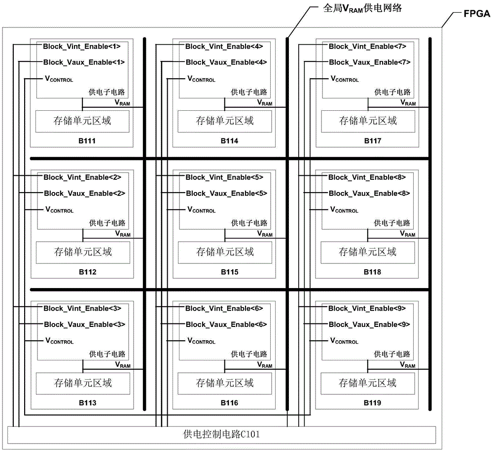
[0072] The present invention will be described by taking the storage unit of the FPGA configuration memory array divided into 9 areas roughly equally according to the boundaries of logic resources as an example.

[0073] Figure 8 It is a block diagram of FPGA, the input and output ports (IOB) are located around the chip, the configurable logic module (CLB) is arranged in an array internally, the block memory (BRAM) is interspersed in the configurable logic module (CLB), and the clock module (of which Including DCM and global clock BUF) are distributed in two corners, the dedicated clock path provides a good clock for configuration logic resources, and also includes configuration logic, configuration interface and power supply control circuit. Figure 8 For illustration, only a small number of Input Output Blocks (IOBs) and Configurable Logic Blocks (CLBs) and Block Memory (BRAM) are shown. The configuration memory array (CSRAM) connected to the various blocks throughou...


PUM


Abstract

The invention discloses a multi-power cell and time distribution electrifying system of an FPGA configuration memory array. A memory cell of the FPGA configuration memory array is divided into a plurality of regions, the regions are sequentially electrified one by one, and therefore the electrifying surge current problem of a large-scale single-particle reinforcing SRAM type FPGA is effectively solved. When the FPGA is electrified, the regions are sequentially electrified through an electrifying control circuit, and therefore an electrifying peak current is decreased. The voltages outputted by all electrifying sub-circuits to the memory cell regions are simultaneously connected to an overall network in parallel, therefore, the voltages of all the memory cell regions of a whole FPGA chip are same, and the consistency is guaranteed. According to the multi-power cell and time distribution electrifying system of the FPGA configuration memory array, the electrifying surge current can be effectively eliminated, and meanwhile scale independence between the electrifying current and the FPGA is achieved by dividing the FPGA into multiple regions.

Description

technical field [0001] The invention relates to a multi-power partition time-sharing power-on system for an FPGA configuration memory array, which belongs to the technical field of integrated circuits. Background technique [0002] A Field Programmable Logic Gate Array (hereinafter referred to as FPGA) can implement different logic functions according to configuration information. The SRAM type FPGA uses a configuration memory array composed of SRAM units to store user configuration information. The configuration frame composed of SRAM units can be programmed repeatedly indefinitely, making the FPGA application very flexible, especially suitable for aerospace engineering. The characteristic requirements of high reliability, multiple varieties, and small batches of devices are widely used in aerospace engineering. [0003] In the prior art, power is supplied to all memory cells at the same time when the configuration memory array is powered on. The disadvantage is that the s...

Claims


Application Information

Patent Timeline
Patent Type & Authority Applications(China)
IPC IPC(8): G11C11/417
CPCG11C11/417
Inventor 陈雷张彦龙李智赵元富张健李学武孙华波
Owner BEIJING MXTRONICS CORP
Why Eureka
Try Eureka