Rapid chip polishing device and method

A polishing device and wafer technology, which is applied to grinding devices, electrical components, circuits, etc., can solve the problems of increased power consumption, different heat, and low temperature of the polishing system. Effect

Active Publication Date: 2016-06-15
SUZHOU SICREAT NANOTECH CO LTD
View PDF10 Cites 2 Cited by
  • Summary
  • Abstract
  • Description
  • Claims
  • Application Information

AI Technical Summary

Problems solved by technology

[0005] But in the above-mentioned double-sided polishing process, because the pressure of the polishing pad to the wafer is small, the heat generated by friction is less, causing the temperature of the whole polishing system to be low, which is not conducive to polishing, and because the material of the polishing pad and the material of the wafer are different. Different, so the same polishing machine produces different heat when using different polishing pads or polishing wafers of different materials under the same polishing conditions
In view of this situation, the advanced polishing machine will introduce an electric heating and polishing device to strictly control the polishing process at a certain temperature, but the large plate will be deformed when heated for a long time, which greatly shortens the life of the large plate and increases power consumption.

Method used


Image

  • Rapid chip polishing device and method
  • Rapid chip polishing device and method
  • Rapid chip polishing device and method

Examples


Embodiment Construction

[0027] The present invention will be further described below in conjunction with specific drawings and embodiments.

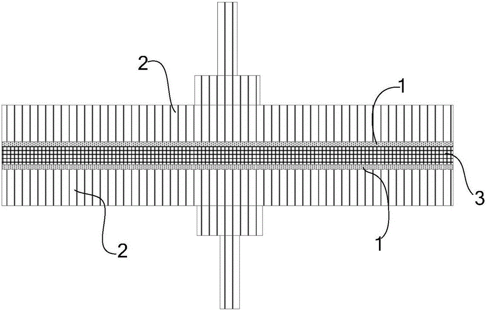
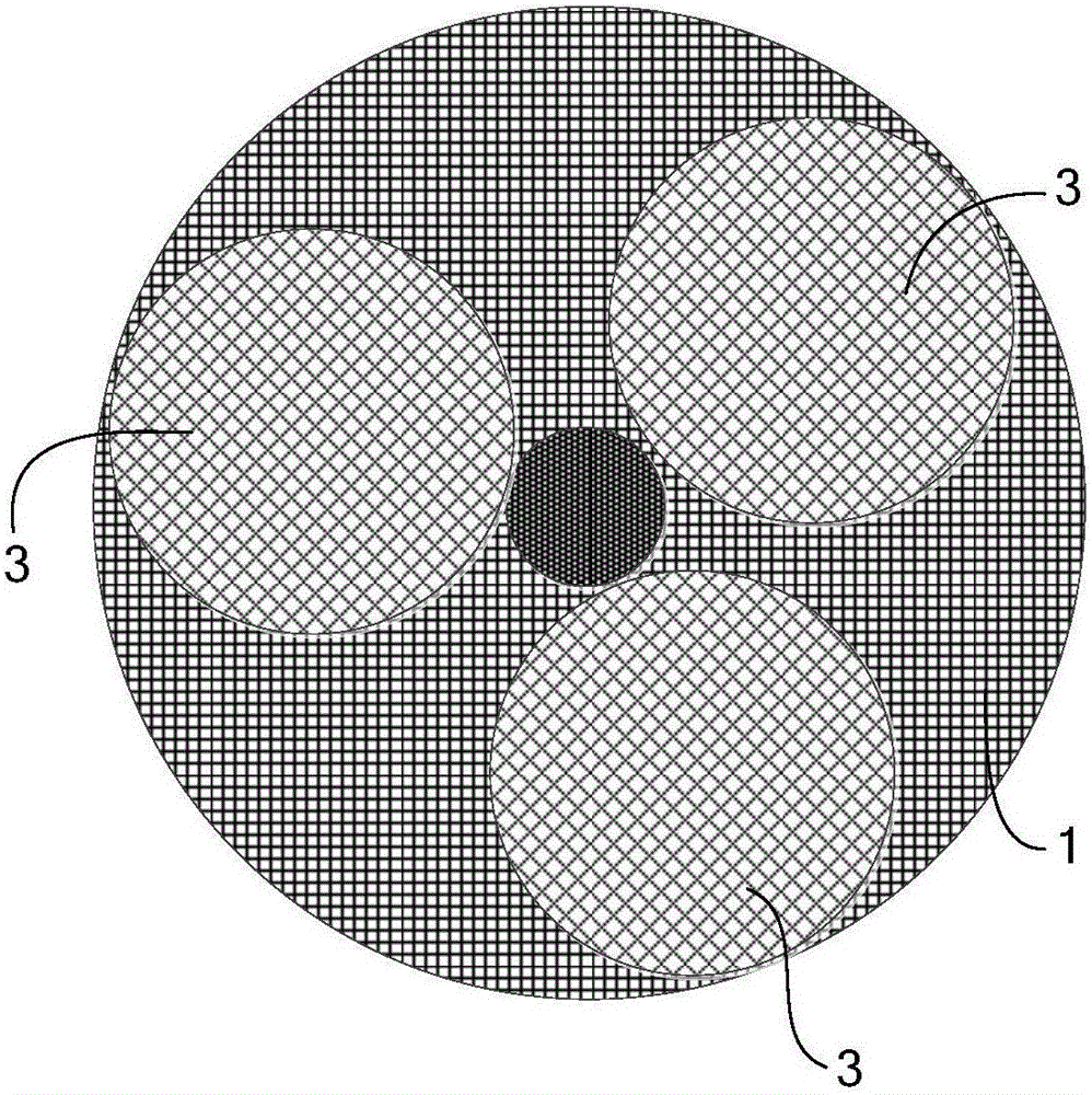
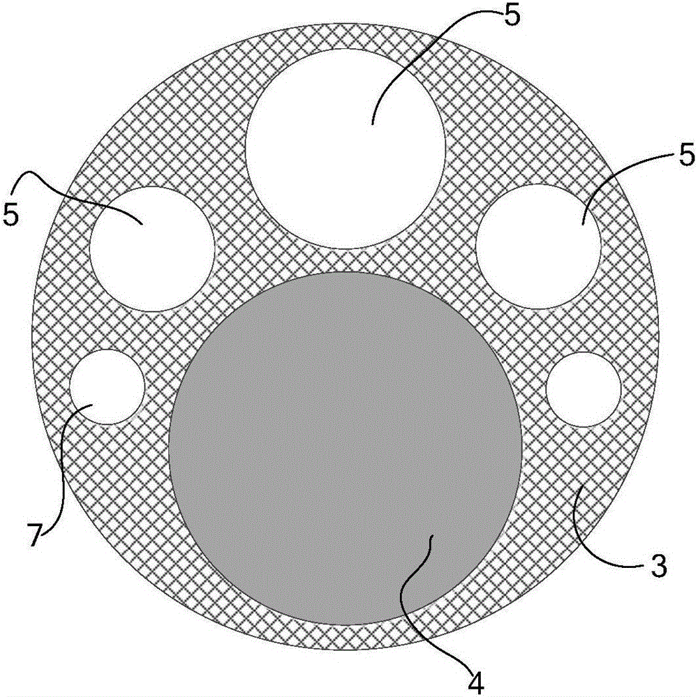
[0028] In order to accurately control the polishing temperature and improve the polishing speed, the present invention includes symmetrically distributed polishing large discs 2, at least one planetary wheel 3 for fixing the wafer 4 is set between the polishing large discs 2, and the polishing large discs 2 and There is a polishing pad 1 between the planetary wheels 3; a heat generating diaphragm 6 for contacting the polishing pad 1 and generating heat when the wafer 4 is polished is arranged in at least one planetary wheel 3 between the polishing large discs 2 .

[0029] Specifically, the polishing platter 2 is symmetrically distributed on both sides of the planetary wheel 3, and the polishing pads 1 are respectively attached to the surface of the polishing platter 2 adjacent to the planetary wheel 3, and a plurality of wafers 4 for polishing are fixed by the p...


PUM


Abstract

The invention relates to a polishing device and method, in particular to a rapid chip polishing device and method, and belongs to the technical field of semiconductor polishing. According to the technical scheme, the rapid chip polishing device comprises big polishing disks distributed symmetrically, at least one swimming star wheel used for fixing a chip is arranged between the big polishing disks, and polishing pads are arranged between the big polishing disks and the swimming star wheels; and at least one swimming star wheel between the big polishing disks is internally provided with a heat generating membrane used for making contact with the corresponding polishing pad and generating heat when the chip is polished. The rapid chip polishing deviceis compact in structure, compatible with the prior art, convenient to use and operate, capable of accurately controlling the polishing temperature and increasing the polishing speed, wide in application range, safe and reliable.

Description

technical field [0001] The invention relates to a polishing device and method, in particular to a wafer rapid polishing device and method, belonging to the technical field of semiconductor polishing. Background technique [0002] Chemical Mechanical Polishing (CMP) technology is one of the key technologies for wafer surface processing. It is widely used in the surface polishing process. [0003] The CMP process is a process in which mechanical and chemical effects are balanced. For example, in the advanced double-sided ultra-thin wafer polishing process, two large plates are used to sandwich the star wheel, and the wafer is fixed on the star wheel. The reverse rotation and the self-rotation of the star wheel drive the wafer to interact with the polishing pad. At this time, the chemically alkaline polishing liquid contacts the surface of the wafer and undergoes a corrosion reaction. The surface of the wafer will be corroded by the alkali solution, and the friction with the p...

Claims


Application Information

Patent Timeline
Patent Type & Authority Applications(China)
IPC IPC(8): B24B37/08B24B37/28B24B37/34H01L21/67
CPCB24B37/08B24B37/28B24B37/34H01L21/67126
Inventor 夏秋良
Owner SUZHOU SICREAT NANOTECH CO LTD
Why Eureka
Try Eureka