Liquid crystal display panel and manufacturing method thereof

A technology of liquid crystal display panels and manufacturing methods, applied in nonlinear optics, instruments, optics, etc., can solve problems such as inability to fundamentally eliminate air bubbles, high production costs, and lower product yield, so as to reduce the risk of color resistance air bubbles and improve The flatness of the film surface and the effect of improving product yield

Active Publication Date: 2016-06-22
SHENZHEN CHINA STAR OPTOELECTRONICS TECH CO LTD
View PDF7 Cites 30 Cited by
  • Summary
  • Abstract
  • Description
  • Claims
  • Application Information

AI Technical Summary

Problems solved by technology

[0005] The main material of the color filter layer 130' is an organic substance. In the prior art, when the color filter layer 130' is manufactured, gas may remain inside it. In a high temperature environment, or when the display is in a vibrating working state, the inside of the color filter layer 130' will slowly release small molecular carbon oxide gases, such as CO, CO 2 etc. After these small molecular gases are generated, they will penetrate the passivation layer on the surface of the color filter layer 130', the first transparent conductive thin layer 140', and the lower alignment film 150', and enter between the lower substrate 100' and the upper substrate 200'. In the interlayer between the liquid

Method used


Image

  • Liquid crystal display panel and manufacturing method thereof
  • Liquid crystal display panel and manufacturing method thereof
  • Liquid crystal display panel and manufacturing method thereof

Examples


Embodiment Construction

[0041] In order to further illustrate the technical means adopted by the present invention and its effects, the following describes in detail in conjunction with preferred embodiments of the present invention and accompanying drawings.

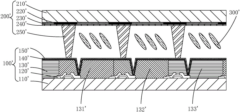
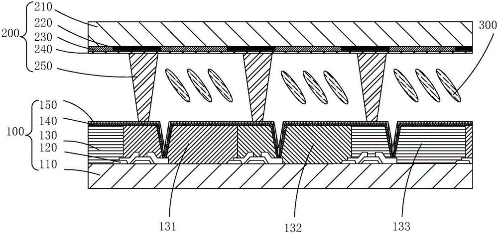
[0042] see Figure 2 to Figure 3 , the present invention provides a liquid crystal display panel: comprising a lower substrate 100 and an upper substrate 200 disposed opposite to each other, and a liquid crystal layer 300 sandwiched between the lower substrate 100 and the upper substrate 200 .

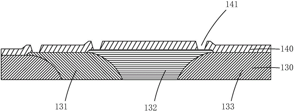
[0043]The liquid crystal display panel of the present invention is a COA liquid crystal display panel, that is, the color filter layer and the TFT array are arranged on the same side. Specifically, the lower substrate 100 includes: a first base substrate 110, a TFT array layer 120 disposed on the first base substrate 110; a color filter layer 130 disposed on the first substrate 110 and the TFT array layer 120 ; the passivation layer 140 disposed on th...


PUM

PropertyMeasurementUnit
Widthaaaaaaaaaa

Abstract

The invention provides a liquid crystal display panel and a manufacturing method thereof.The liquid crystal display panel is of a COA-type structure, a color light filter layer comprises a plurality of color stopping units connected in sequence, every two adjacent color stopping units are partially superposed at the junction position, a passivation layer on the color light filter layer is provided with holes at the upper portions of the superposed positions of the corresponding every two adjacent color stopping units, accordingly micro-molecular gas in the color light filter layer can be released out in the manufacturing process of the passivation layer and the follow-up manufacturing process of transparent conductive layer crystals, the risk of color stopping bubbles is reduced, meanwhile the heights of the superposed positions of color stopping are decreased, the flatness is improved, and the higher product yield is obtained.According to the manufacturing method of the liquid crystal display panel, the holes are formed in the upper portions of the superposed positions of every two adjacent color stopping units, corresponding to the inside of the color light filter layer, on the passivation layer, the risk of color stopping bubbles is reduced on the premise that the manufacturing process and the cost are not increased additionally, meanwhile the heights of the superposed positions of color stopping are decreased, the improvement of the flatness is promoted, and the product yield is improved.

Description

technical field [0001] The invention relates to the technical field of liquid crystal display, in particular to a liquid crystal display panel and a manufacturing method thereof. Background technique [0002] A liquid crystal display (Liquid Crystal Display, LCD) is one of the most widely used flat panel displays at present, and a liquid crystal panel is a core component of the liquid crystal display. [0003] A traditional liquid crystal panel is usually composed of a color filter (ColorFilter, CF) substrate, a thin film transistor array substrate (ThinFilmTransistorArraySubstrate, TFTArraySubstrate), and a liquid crystal layer (LiquidCrystalLayer) arranged between the two substrates. Liquid crystal molecules are placed between two parallel glass substrates. There are many small vertical and horizontal wires between the two glass substrates. The direction of the liquid crystal molecules is controlled by electrifying or not, and the light from the backlight module is refract...

Claims


Application Information

Patent Timeline
IPC IPC(8): G02F1/1362G02F1/1335G02F1/13
CPCG02F1/1303G02F1/133514G02F1/133516G02F1/1362G02F1/136222
Inventor 谢子清谢克成
Owner SHENZHEN CHINA STAR OPTOELECTRONICS TECH CO LTD
Why Eureka
Try Eureka