
Method for assignment of multiple power supply pins of voltage island

A distribution method and technology of voltage island, applied in electrical digital data processing, CAD circuit design, special data processing applications, etc., can solve the circuit failure of circuit macro-modules, the voltage drop does not meet the design constraints, and affects the voltage drop of power supply network nodes, etc. problem, to achieve the effect of optimizing the voltage drop and reducing the design cost

Active Publication Date: 2016-06-22
NINGBO UNIV
View PDF3 Cites 1 Cited by
  • Summary
  • Abstract
  • Description
  • Claims
  • Application Information

AI Technical Summary

Problems solved by technology

[0004] The position of the power supply pin directly affects the voltage drop of the power supply network node of the voltage island in the multi-voltage chip. If the distribution is improper, the voltage drop will inevitably fail to meet the design constraints, so that the insufficient power supply of the circuit macromodule in the voltage island will cause the circuit to fail.
In addition, in order to meet the voltage drop constraints, the wiring area consumed by the power network will also increase accordingly.

Method used


Image

  • Method for assignment of multiple power supply pins of voltage island
  • Method for assignment of multiple power supply pins of voltage island
  • Method for assignment of multiple power supply pins of voltage island

Examples


Embodiment Construction

[0030] The present invention will be further described in detail below in conjunction with the accompanying drawings and embodiments.

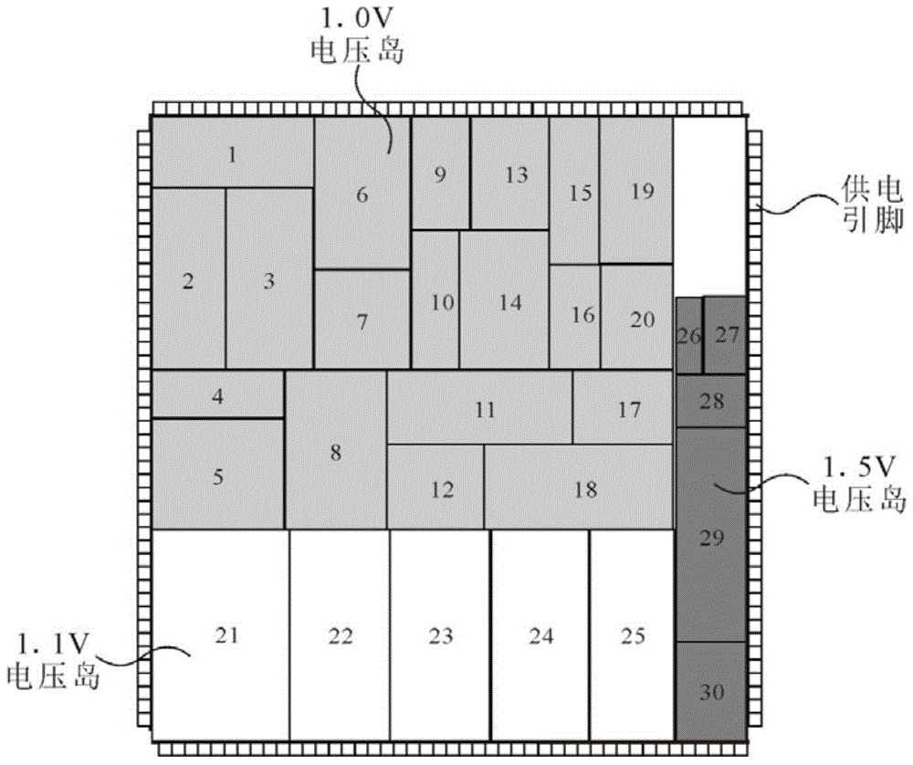
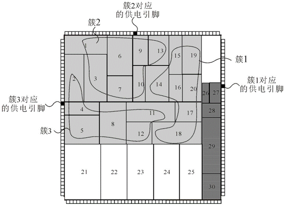
[0031] Taking a chip containing three voltage islands as an example, its layout representation is shown in figure 1 , figure 1 That is, a schematic layout diagram of a circuit macromodule including three voltage islands, which contains 30 circuit macromodules, namely b 1 , b 2 , b 3 ,...,b 30 , the multi-supply pin allocation method of its voltage island, including the following steps:

[0032] Step ①: Define a voltage island as an area composed of circuit macromodules operating at the same operating voltage and occupying a continuous two-dimensional physical space. The chip is composed of several voltage islands. figure 1 Contains three voltage islands, where the circuit macroblock b 1 ~b 20 A voltage island with a working voltage of 1.0V is formed, and the circuit macromodule b 21~b 25 A voltage island with a working voltage of 1.1V...


PUM


Abstract

The invention discloses a method for assignment of multiple power supply pins of a voltage island. The method comprises the following steps of firstly, adopting a Kmeans assembly algorithm to divide a circuit macroblock included in the voltage island into n clusters based on the coordinate information of the circuit macro-blocks according to the physical information of the voltage island; secondly, carrying out fine tuning on ownership of the circuit micro-blocks in all clusters in order to enable the power density of each cluster to be approximately equal; and lastly, assigning different stiffness coefficients to springs connected to the circuit micro-blocks according to the current density, determining the position of an energy balance point of a spring system and completing assignment of the power supply pins of the circuit micro-blocks included in each cluster, and repeating the process to complete assignment of multiple power supply pins required by all voltage islands. According to the method, the voltage drop of nodes of a power network of the voltage island on a chip can be quickly and effectively optimized, so that the an automatic design optimization method for assignment of the power supply pins of the voltage island on the chip is enriched, and the design cost is reduced. Through example verification, the voltage drop of the power network, which is obtained by the method, can be effectively reduced.

Description

technical field [0001] The invention relates to an automatic design method of an on-chip system, in particular to a method for allocating multiple power supply pins of a voltage island. Background technique [0002] The dynamic power consumption of integrated circuits is proportional to the square of the power supply voltage, and the static power consumption is also proportional to the voltage. Therefore, reducing the power supply voltage of the chip is considered to be the most effective and direct low-power design method. The multi-voltage technology is based on this principle, supplying higher voltage to key circuit macro modules (hereinafter referred to as modules) in the chip to ensure the performance of the chip; and supplying lower voltage to non-critical modules to save power consumption. In order to reduce the complexity of power network design, modules working at the same operating voltage are often gathered in a continuous physical space to form a voltage island (...

Claims


Application Information

Patent Timeline
IPC IPC(8): G06F17/50
CPCG06F30/39
Inventor 储著飞夏银水王伦耀
Owner NINGBO UNIV
Learn More