Thin film transistor and preparation method thereof, array substrate and display device

A technology of thin-film transistors and array substrates, applied in the display field, can solve problems such as impacting, reducing the response speed of the display, and increasing the load of the display

Active Publication Date: 2016-06-22
CHONGQING BOE OPTOELECTRONICS +1
View PDF3 Cites 11 Cited by
  • Summary
  • Abstract
  • Description
  • Claims
  • Application Information

AI Technical Summary

Problems solved by technology

However, the above-mentioned overlapping region A causes parasitic capacitance to be formed inside the TFT, which will adversely affect the display performance, such as increasing the display load, reducing the response speed of the

Method used


Image

  • Thin film transistor and preparation method thereof, array substrate and display device
  • Thin film transistor and preparation method thereof, array substrate and display device
  • Thin film transistor and preparation method thereof, array substrate and display device

Examples


Embodiment 1

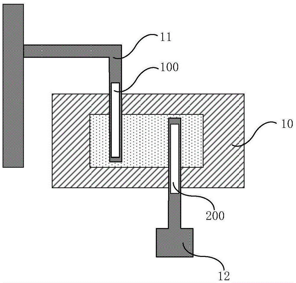
[0043] In this example, if Figure 4a The source 11 of the shown TFT includes a U-shaped first working portion 110 . The drain 12 includes a strip-shaped second working portion 120 .

[0044] In this case, the first opening part 100 is a U-shaped through hole, and a U-shaped through hole is provided on the above-mentioned one U-shaped first working part 110 along the outline of the first working part 110 . In this way, only one U-shaped through hole needs to be prepared on the first working portion 110 to reduce the overlapping area between the source electrode 11 and the gate 10 without preparing multiple through holes. In addition, the above-mentioned U-shaped through hole is provided along the outline of the first working portion 110 , so that the overlapping area between the source electrode 11 and the gate electrode 10 can be minimized through one patterning process.

[0045] Preferably, the distance H1 from the inner side C1 of the U-shaped first working portion 110 to...

Embodiment 2

[0050] In this embodiment, the source 11 of the TFT is the same as the first embodiment, including a U-shaped first working portion 110 . Drain 12 as Figure 4b Shown includes a U-shaped second working portion 120 .

[0051] In this case, the setting method of the first opening 100 is the same as that of the first embodiment, and will not be repeated here.

[0052] The second opening 200 is a U-shaped through hole, and a U-shaped through hole is provided on the second working part 120 along the outline of the second working part 120 . In this way, only one U-shaped through hole needs to be prepared on the second working portion 120 to reduce the overlapping area between the drain 12 and the gate 10 without preparing multiple through holes. In addition, the above-mentioned U-shaped through holes are provided along the outline of the second working portion 120 , which can minimize the overlapping area between the drain 12 and the gate 10 through one patterning process.

[005...

Embodiment 3

[0055] In this example, if Figure 4c As shown, the source 11 of the TFT includes two U-shaped first working portions 110 . The drain 12 includes two strip-shaped second working portions 120 .

[0056] In this case, the first opening 100 is a U-shaped through hole, and each U-shaped first working part 110 in the source 11 is provided with a U-shaped through hole along the outline of the first working part 110 . In this way, it is only necessary to prepare a U-shaped through hole on each first working part 110 to reduce the overlapping area between the source electrode 11 and the gate 10, without preparing a U-shaped through hole on each first working part 110. Multiple vias. In addition, the above-mentioned U-shaped through hole is provided along the outline of the first working portion 110 , so that the overlapping area between the source electrode 11 and the gate electrode 10 can be minimized through one patterning process.

[0057] Preferably, the distance H1 from the in...


PUM


Abstract

One embodiment of the invention provides a thin film transistor and a preparation method thereof, an array substrate and a display device, and relates to the technical field of display, reducing the self-stray capacitance of the TFT. The thin film transistor comprises a grid electrode, a source electrode and a drain electrode, wherein a first opening part is formed on the grid electrode/or the source electrode, and the first opening part is positioned at least at an overlapping area of the grid electrode and the source electrode; an/or, a second opening part is formed on the grid and / or the drain electrode, and the second opening part is positioned at least at the overlapping area of the grid electrode and the drain electrode.

Description

technical field [0001] The invention relates to the field of display technology, in particular to a thin film transistor, a preparation method thereof, an array substrate and a display device. Background technique [0002] In the field of display technology, LCD (Liquid Crystal Display, liquid crystal display) and OLED (Organic Light Emitting Diode, organic light emitting diode) displays are provided with TFT (Thin Film Transistor, thin film transistor) for controlling the display of pixels. Therefore, the performance of the TFT becomes one of the key factors affecting the display performance of the display. [0003] In the prior art, the structure of TFT is as figure 1 As shown, it includes a gate 10 and a source 11 and a drain 12 arranged in different layers from the gate 10 . Wherein, in order to enable the TFT to have switching performance, the gate 10 needs to have an overlapping area A1 with the source 11 , and the gate 10 needs to have an overlapping area A2 with th...

Claims


Application Information

Patent Timeline
IPC IPC(8): H01L27/12H01L29/417H01L29/423H01L29/66H01L29/786
CPCH01L27/1214H01L29/41733H01L29/42384H01L29/66742H01L29/786H01L29/78618
Inventor 齐智坚杨妮余道平顾可可侯宇松刘信陈帅苟中平
Owner CHONGQING BOE OPTOELECTRONICS
Why Eureka
Try Eureka