Terahertz quantum level cascaded laser with integration of absorption waveguide and fabrication method of terhertz quantum level cascaded laser
A technology of quantum cascade and fabrication method, which is applied to semiconductor lasers, lasers, phonon exciters, etc., can solve the problems such as the large difference between the materials used and THzQCL, and the inability to use integrated systems, so as to improve the absorption efficiency, and the preparation process is simple and flexible. , the effect of high waveguide loss
- Summary
- Abstract
- Description
- Claims
- Application Information
AI Technical Summary
Problems solved by technology
Method used
Image
Examples
Embodiment 1
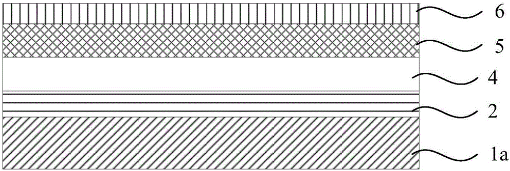
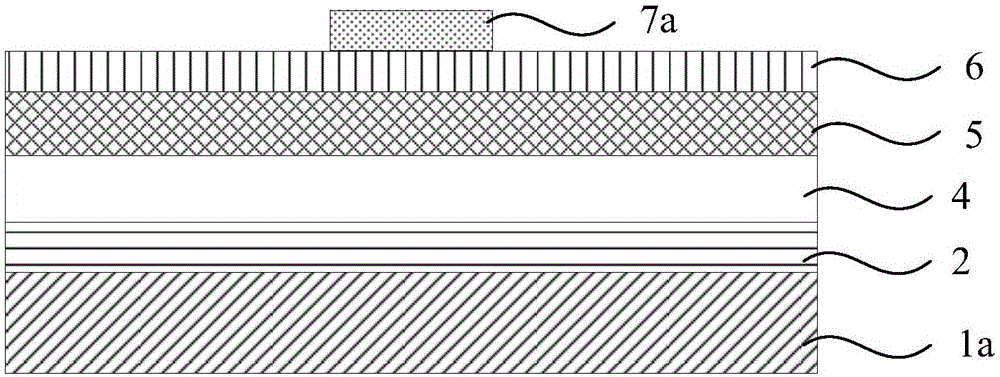
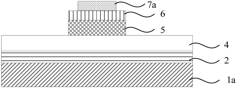
[0083] Such as Figure 1 to Figure 9 As shown, the terahertz quantum cascade laser with integrated absorption waveguide includes:
[0084] Semi-insulating GaAs substrate 1a;
[0085] a GaAs buffer layer 2 located on the upper surface of the semi-insulating GaAs substrate 1a;
[0086] An n-type heavily doped lower contact layer 4 located on the surface of the GaAs buffer layer 2;
[0087] The active region 5 located on the surface of the n-type heavily doped lower contact layer 4;
[0088] An n-type heavily doped upper contact layer 6 located on the surface of the active region 5;
[0089] The first and second upper electrode metal layers 7a and 7b are located on the surface of the n-type heavily doped upper contact layer 6 and are separated by a distance L, wherein the second upper electrode metal layer 7b can be formed after annealing. The upper electrode metal layer of the waveguide loss;
[0090] And the lower electrode metal layer 8 located on the surface of the n-typ...
Embodiment 2
[0127] The present invention also provides a terahertz quantum cascade laser with an integrated absorption waveguide. The terahertz quantum cascade laser with an integrated absorption waveguide includes:
[0128] doped GaAs substrate 1b;
[0129] a bonding metal layer 3 located on the upper surface of the doped GaAs substrate 1b;
[0130] An n-type heavily doped lower contact layer 4 located on the surface of the bonding metal layer 3;
[0131] The active region 5 located on the surface of the n-type heavily doped lower contact layer 4;
[0132] An n-type heavily doped upper contact layer 6 located on the surface of the active region 5;
[0133] And the first and second upper electrode metal layers 7a, 7b located on the surface of the n-type heavily doped upper contact layer 6 and provided with a distance L, wherein the second upper electrode metal layer 7b can be formed after annealing High waveguide loss top electrode metal layer.
[0134] It should be noted that the fir...
PUM
 Abstract
Description
Claims
Application Information


