A One-bit Full Adder Based on Finfet Device

A full adder, the eleventh technology, applied in logic circuits with logic functions, etc., can solve the problems of extremely narrowed CMOS transistor space, increased device leakage current, and limited circuit performance, so as to eliminate static power consumption and power consumption. The time-consuming delay product is small and the effect of reducing the delay

Active Publication Date: 2018-08-14
NINGBO UNIV
View PDF3 Cites 0 Cited by
  • Summary
  • Abstract
  • Description
  • Claims
  • Application Information

AI Technical Summary

Problems solved by technology

[0002] With the continuous reduction of transistor size, limited by the short channel effect and the current manufacturing process, the space for reducing the size of ordinary CMOS transistors is extremely narrow
When the size of ordinary CMOS transistors is reduced to below 20nm, the leakage current of the device will increase sharply, resulting in large leakage power consumption of the circuit
Moreover, the short-channel effect of the circuit becomes more obvious, and the device becomes quite unstable, which greatly limits the improvement of the circuit performance

Method used


Image

  • A One-bit Full Adder Based on Finfet Device
  • A One-bit Full Adder Based on Finfet Device
  • A One-bit Full Adder Based on Finfet Device

Examples


Embodiment 1

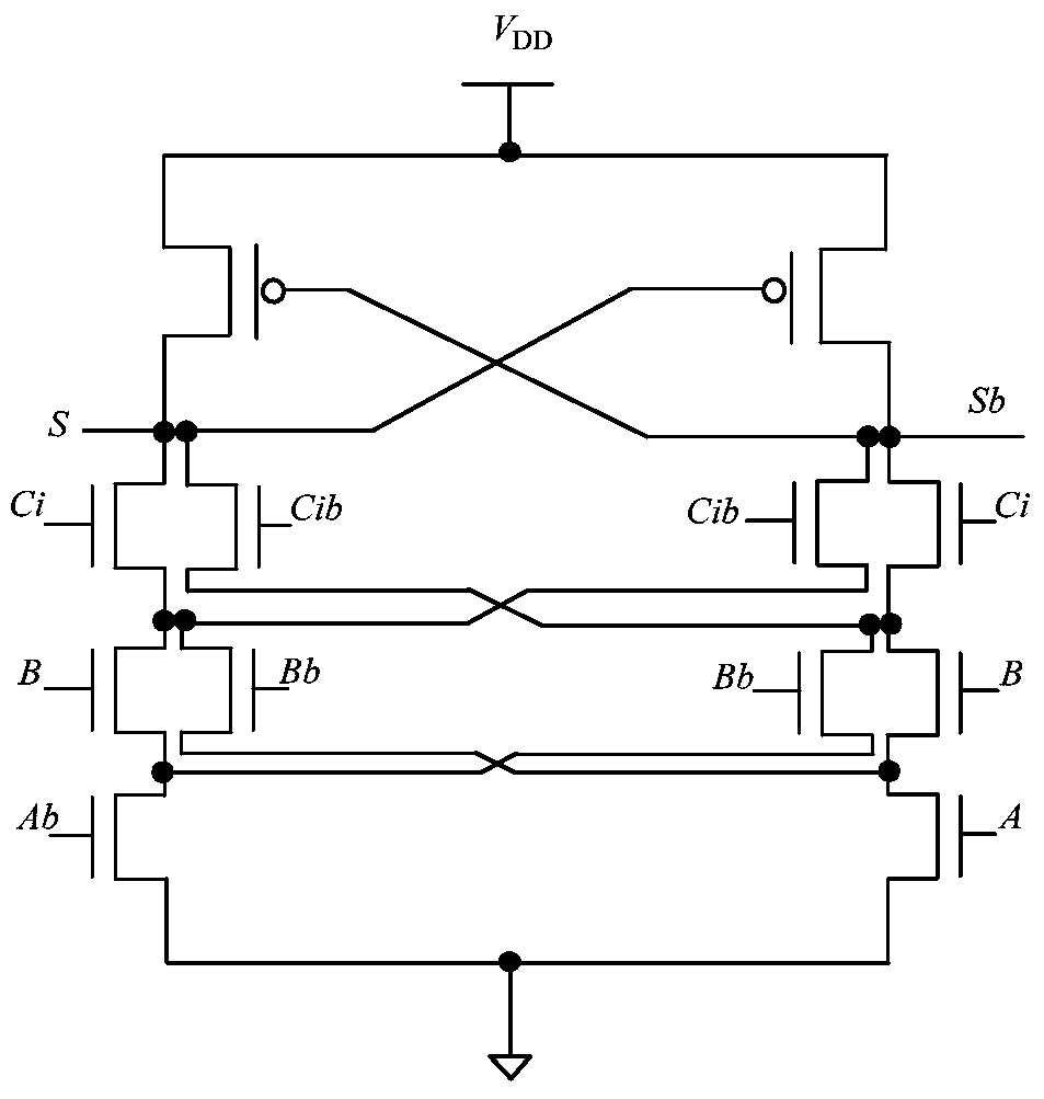
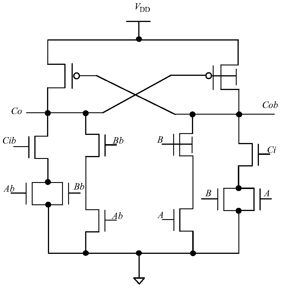
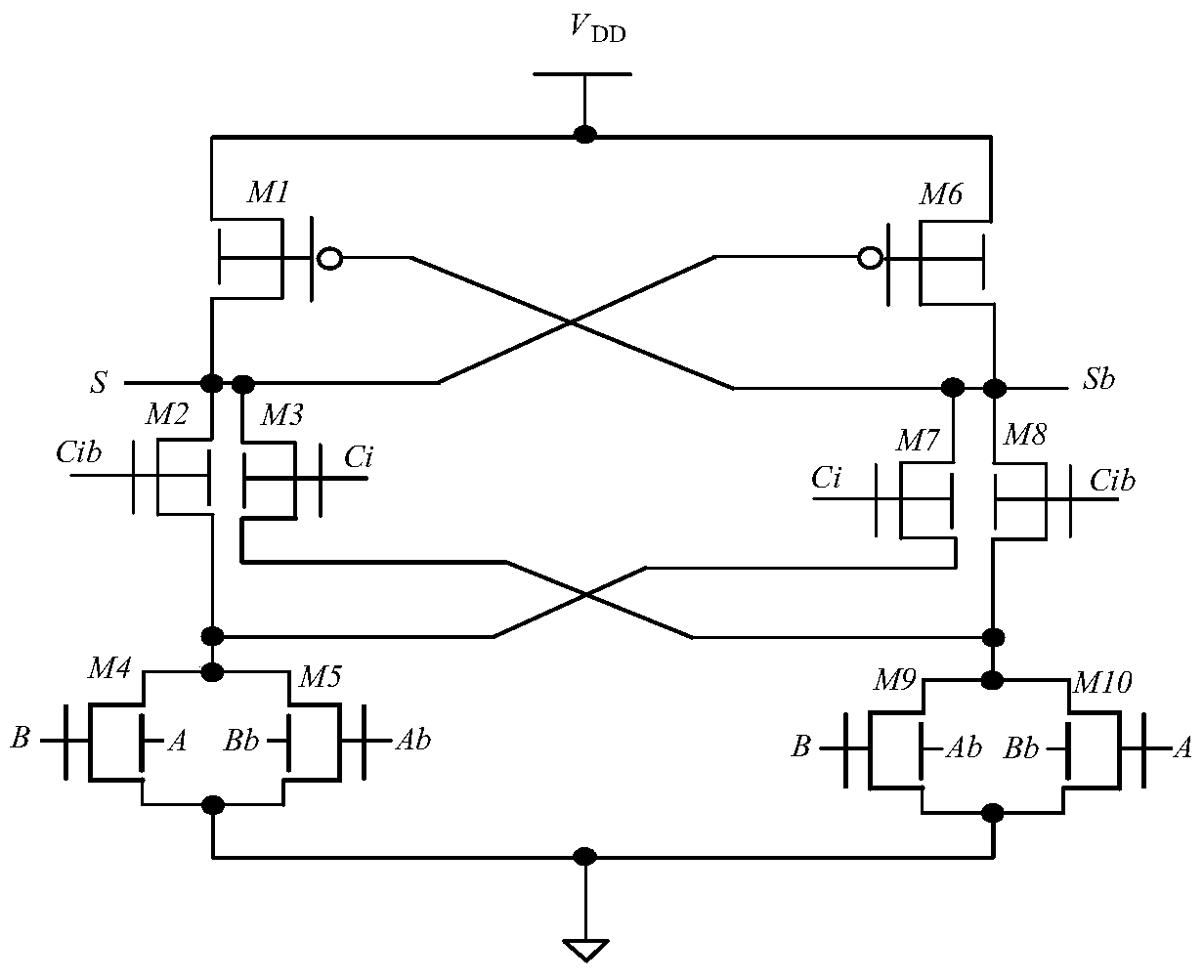
[0018] Embodiment one: as shown in Fig. 2 (a) and Fig. 2 (b), a kind of full adder based on FinFET device comprises summing output circuit and carry output circuit; Summing output circuit comprises the first FinFET tube M1, the second FinFET tube M2, the third FinFET tube M3, the fourth FinFET tube M4, the fifth FinFET tube M5, the sixth FinFET tube M6, the seventh FinFET tube M7, the eighth FinFET tube M8, the ninth FinFET tube M9 and The tenth FinFET tube M10, the first FinFET tube M1 and the sixth FinFET tube M6 are P-type FinFET tubes, the second FinFET tube M2, the third FinFET tube M3, the fourth FinFET tube M4, the fifth FinFET tube M5, and the seventh FinFET tube M5. The FinFET tube M7, the eighth FinFET tube M8, the ninth FinFET tube M9 and the tenth FinFET tube M10 are all N-type FinFET tubes, the first FinFET tube M1, the second FinFET tube M2, the third FinFET tube M3, and the sixth FinFET tube M6, the seventh FinFET tube M7 and the eighth FinFET tube M8 are all lo...

Embodiment 2

[0020]Embodiment two: as shown in Fig. 2 (a) and Fig. 2 (b), a kind of full adder based on FinFET device comprises summing output circuit and carry output circuit; Summing output circuit comprises the first FinFET tube M1, the second FinFET tube M2, the third FinFET tube M3, the fourth FinFET tube M4, the fifth FinFET tube M5, the sixth FinFET tube M6, the seventh FinFET tube M7, the eighth FinFET tube M8, the ninth FinFET tube M9 and The tenth FinFET tube M10, the first FinFET tube M1 and the sixth FinFET tube M6 are P-type FinFET tubes, the second FinFET tube M2, the third FinFET tube M3, the fourth FinFET tube M4, the fifth FinFET tube M5, and the seventh FinFET tube M5. The FinFET tube M7, the eighth FinFET tube M8, the ninth FinFET tube M9 and the tenth FinFET tube M10 are all N-type FinFET tubes, the first FinFET tube M1, the second FinFET tube M2, the third FinFET tube M3, and the sixth FinFET tube M6, the seventh FinFET tube M7 and the eighth FinFET tube M8 are all low...


PUM


Abstract

The invention discloses a one-bit full adder based on FinFET devices. The one-bit full adder comprises a sum output circuit and a carry output circuit, the sum output circuit comprises a first FinFET transistor, a second FinFET transistor, a third FinFET transistor, a fourth FinFET transistor, a fifth FinFET transistor, a sixth FinFET transistor, a seventh FinFET transistor, an eighth FinFET transistor, a ninth FinFET transistor, and a tenth FinFET transistor, and the carry output circuit comprises an eleventh FinFET transistor, a twelfth FinFET transistor, a thirteenth FinFET transistor, a fourteenth FinFET transistor, a fifteenth FinFET transistor, a sixteenth FinFET transistor, a seventeenth FinFET transistor, and an eighteenth FinFET transistor. The one-bit full adder is advantageous in that the sum output circuit and the carry output circuit both employs the differential circuits, sum output and carry output are realized via alternative work, and the one-bit adder works in a differential manner so that the static power consumption of the circuits can be completely eliminated; besides, opposite logic output is realized, an extra inverter is not needed for opposite logic so that the number of the transistors is further reduced, the circuit area is small, the time delay is short, the power consumption is low, and the consumption-delay product is small.

Description

technical field [0001] The invention relates to a one-bit full adder, in particular to a one-bit full adder based on a FinFET device. Background technique [0002] As the size of transistors continues to shrink, limited by the short-channel effect and the current manufacturing process, the space for reducing the size of ordinary CMOS transistors is extremely narrowed. When the size of an ordinary CMOS transistor is reduced to below 20nm, the leakage current of the device will increase sharply, resulting in a large leakage power consumption of the circuit. Moreover, the short-channel effect of the circuit becomes more obvious, and the device becomes quite unstable, which greatly limits the improvement of the circuit performance. FinFET tube (Fin Field-Effect Transistor, Fin Field-Effect Transistor) is a new complementary metal oxide semiconductor (CMOS) transistor is a new type of 3D transistor, the channel of the FinFET tube is zero-doped or low-doped The channel is surrou...

Claims


Application Information

Patent Timeline
Patent Type & Authority Patents(China)
IPC IPC(8): H03K19/20
CPCH03K19/20
Inventor 胡建平张绪强
Owner NINGBO UNIV
Why Eureka
Try Eureka