PDMS elastomer micro-nano processing method based on crosslinking control control transfer printing

A technology of micro-nano processing and controlled transfer, which is applied in the process of producing decorative surface effects, manufacturing micro-structure devices, micro-structure technology, etc., can solve the problem of limited processing forms, limited micro-nano processing technology, and difficulty in preparing complex and fine materials. Surface pattern structure and other issues, to achieve the effect of a wide range of applications

Inactive Publication Date: 2016-07-06
TIANJIN UNIV
View PDF7 Cites 5 Cited by
  • Summary
  • Abstract
  • Description
  • Claims
  • Application Information

AI Technical Summary

Problems solved by technology

However, the current micro-nano processing technology of PDMS elastomers is very limited, and it is limited by the processing form, and it is difficult to prepare complex and fine surface pattern structures.

Method used


Image

  • PDMS elastomer micro-nano processing method based on crosslinking control control transfer printing
  • PDMS elastomer micro-nano processing method based on crosslinking control control transfer printing
  • PDMS elastomer micro-nano processing method based on crosslinking control control transfer printing

Examples


Embodiment 1

[0016] Embodiment 1: prepare the PDMS membrane of surface patterning, the steps are as follows:

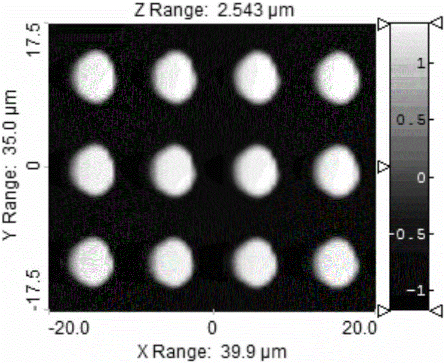
[0017] Step 1, using replica molding method to prepare PDMS with surface microstructure as a stamp for transfer printing: first, mix PDMS prepolymer and crosslinking agent Sylgard184 (purchased from Dow Corning, USA) in a mass ratio of 10:1, Stir well with a glass rod to form a uniform pre-polymer; after degassing the above-mentioned pre-polymer in a circulating water multi-purpose vacuum pump for 1 hour, pour it on a silicon formwork (ie, a master formwork) with a cylindrical array, and the pouring thickness is about 1mm; cured by heating at 70°C for 4h; carefully peel off the PDMS film on the silicon template to form a PDMS stamp, and the PDMS with surface microstructure prepared by the replication molding method (10:1) The surface structure of the stamp is as figure 1 shown.

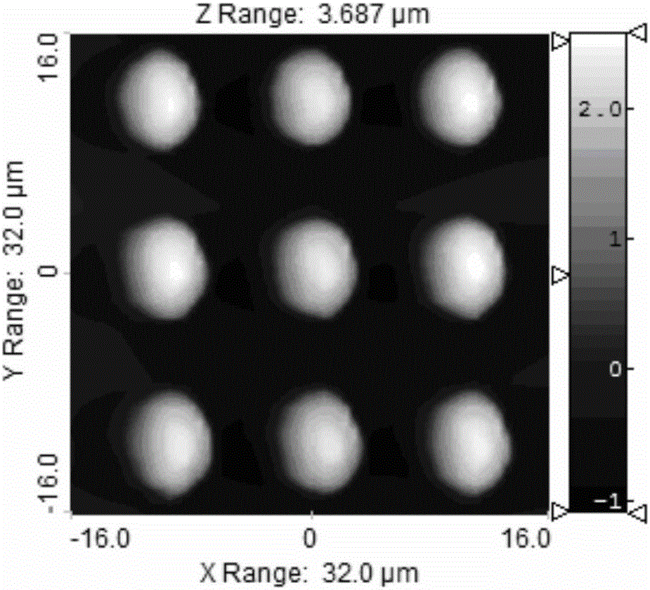
[0018] Step 2, utilizing the pouring method to prepare a PDMS thick film with a thickness of about 1...

Embodiment 2

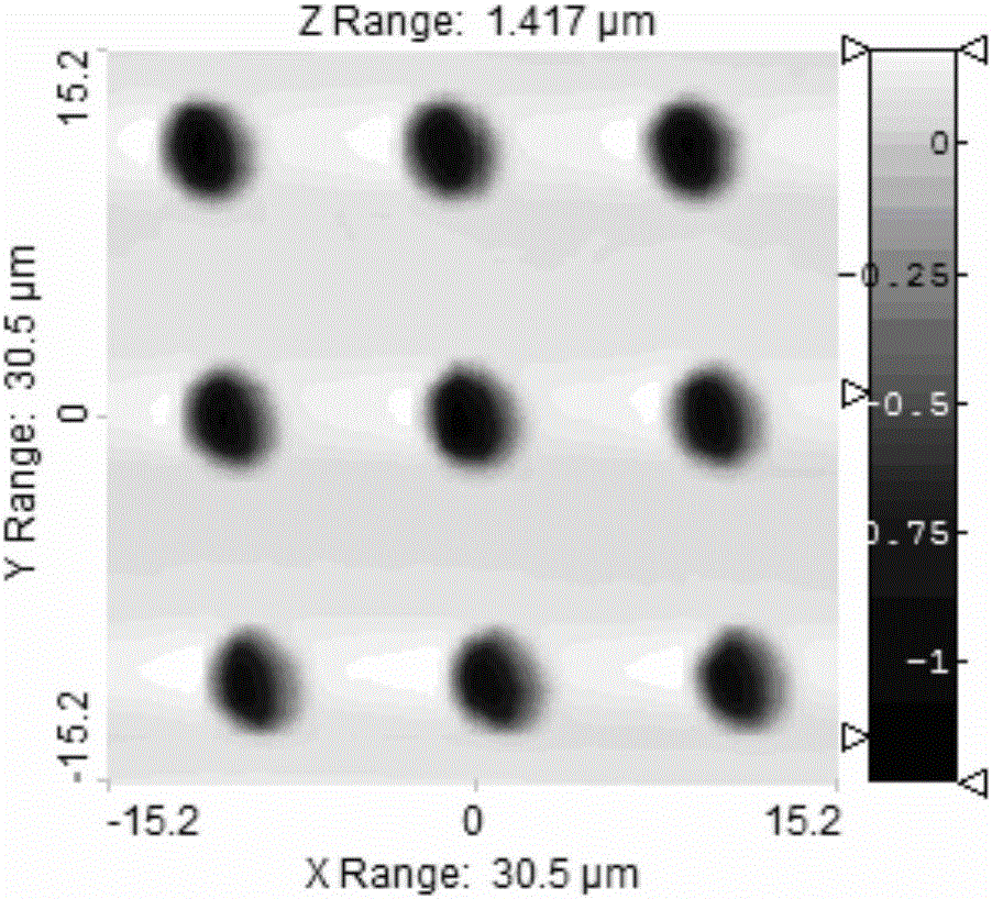
[0021] Embodiment 2: prepare the PDMS membrane of surface patterning, preparation process is basically the same as embodiment 1, the only difference is that the mass ratio of PDMS prepolymer and cross-linking agent in step 1 is changed to 20:1, and the mass ratio in step 2 is changed to 20:1. The mass ratio of PDMS prepolymer and cross-linking agent was changed to 10:1, that is, the cross-linking parameters were determined by PDMS (10:1) / PDMS (20:1) Change to PDMS (20:1) / PDMS (10:1) , the finally obtained PDMS membrane with a regular dot raised pattern on the surface is as follows image 3 The atomic force diagram of .

[0022] As above, by changing the cross-linking agent content in the preparation process, that is, the cross-linking parameters, such as: it can be PDMS (10:1) / PDMS (20:1) 、PDMS (10:1) / PDMS (30:1) 、PDMS (20:1) / PDMS (5:1) 、PDMS (20:1) / PDMS (10:1) any group in .

[0023] In summary, the method of the present invention mainly utilizes the differe...


PUM


Abstract

The invention discloses a PDMS elastomer micro-nano processing method based on crosslinking control control transfer printing. The PDMS elastomer micro-nano processing method comprises the following steps: preparing a PDMS film to serve as a transfer printing substrate by using a pouring method; preparing a PDMS film with a surface microstrucutre to serve as a transfer printing stamp by using a replica casting method; importing a cohesive energy (soft / hard) difference between the PDMS stamp and the planar PDMS substrate by different crosslinking agent contents in the process of preparing the substrate and the stamp; and simultaneously carrying out an OP treatment on the prepared substrate and the stamp for 0.5 min, immediately adhering the substrate and the stamp, and carrying out a heating treatment to improve the contact adhesion of the substrate and the stamp, taking off the stamp, generating cohesive energy breakage on the soft party during the separation to transfer PDMS ink to the hard party, so as to obtain a PDMS film with concave or convex patterns on the surface. The PDMS elastomer micro-nano processing method disclosed by the method is simple and convenient to operate, low in cost, and is used for avoiding the defects of limited applicable range of other related technology and simple processing patterns.

Description

technical field [0001] The invention relates to the micro-nano processing technology of soft matter, in particular to a process method for patterning the surface of PDMS by using a cross-linking control transfer printing method. Background technique [0002] Polydimethylsiloxane (PDMS) is one of the most widely used silicon-based organic polymer materials. As a kind of silicone rubber, PDMS has many uses in outdoor insulation materials, caulking agents, lubricants, human body plastic implants, etc., and more importantly, it has a unique application prospect in micro-nano manufacturing. On the micro / nano scale, PDMS thick / thin films are widely used in soft etching technology, micro / nano fluid control, micro / nano electromechanical systems, biosensing and many other fields. These applications all rely on the surface microstructuring of PDMS. However, the current micro-nano processing technology of PDMS elastomers is very limited, and it is limited by the processing form, and ...

Claims


Application Information

Patent Timeline
Patent Type & Authority Applications(China)
IPC IPC(8): B81C1/00
CPCB81C1/0046
Inventor 鲁从华汪娟娟
Owner TIANJIN UNIV
Why Eureka
Try Eureka