PDMS elastomer micro-nano processing method based on surface oxidation control transfer printing
A technology for controlled transfer and surface oxidation, which is applied in the process of producing decorative surface effects, manufacturing microstructure devices, microstructure technology, etc. Limited technology and other issues, to achieve the effect of a wide range of applications
- Summary
- Abstract
- Description
- Claims
- Application Information
AI Technical Summary
Problems solved by technology
Method used
Image
Examples
Embodiment 1
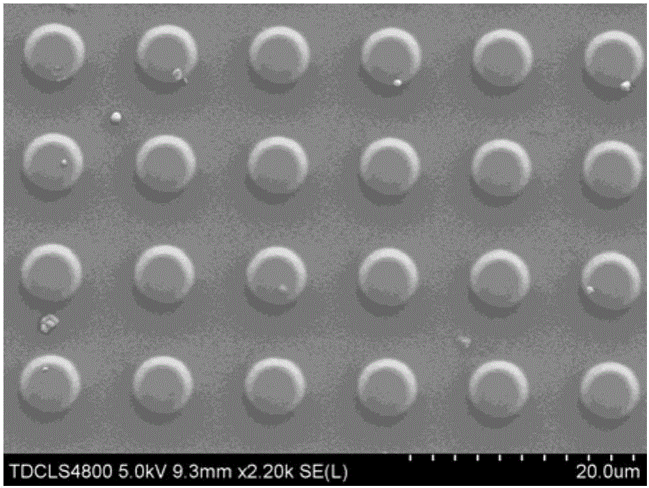
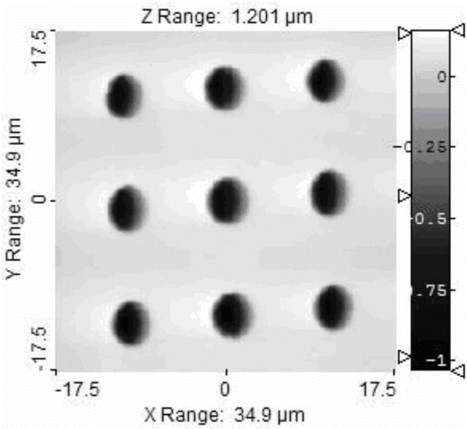
[0023] Embodiment 1, the preparation of the PDMS membrane of surface micro-nano level patterning, the steps are as follows:
[0024] Step 1, utilizing the pouring method to prepare a PDMS thick film with a thickness of about 1mm as the substrate for transfer printing; the specific content is: first, the PDMS prepolymer and crosslinking agent Sylgard184 (purchased from Dow Corning, USA) are 10 in mass ratio: 1. Mix and stir well with a glass rod to form a uniform pre-polymer; degas the above-mentioned pre-polymer in a circulating water multi-purpose vacuum pump for 1 hour, then pour it into a watch glass with a pouring thickness of about 1mm; heat at 70°C 4h for curing; obtain PDMS thick film substrate;
[0025] Step 2: Prepare PDMS with surface microstructure as a stamp for transfer printing by replica molding method; first, mix PDMS prepolymer and crosslinking agent at a mass ratio of 10:1, and fully stir with a glass rod to form a uniform Pre-polymer; after degassing the ab...
Embodiment 2
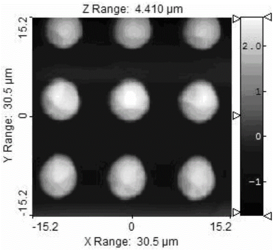
[0029] Embodiment 2: The preparation of the PDMS membrane of surface micro-nano-level patterning, its preparation process is basically the same as embodiment 1, the only difference is that in step 3, it is changed to: the PDMS stamp obtained in step 2 is not subjected to surface oxidation treatment. The PDMS thick film substrate obtained in step 1 is subjected to OP treatment for 30 minutes, and the oxidation treatment parameter of this step is recorded as OP0min / OP30min, and the finally obtained PDMS thick film substrate with a regular dot raised pattern on the surface is as follows: image 3 The atomic force diagram of .
Embodiment 3
[0030] Embodiment 3: the preparation of the PDMS membrane of surface micro-nano scale patterning, its preparation process is as follows:
[0031] Step 1. Prepare a PDMS film with a thickness of about 70nm as a substrate for transfer printing by spin coating. The mass ratio of PDMS to PDMS is 80:1, add n-hexane solution, shake well; use a pipette to take 50 μl of the mixed solution, drop it on a clean cover glass, and spin-coat to form a film at a speed of 6000r / min for 150s; at 95°C Under heating for 1 h to cure; obtain a PDMS film substrate.
[0032] Step 2 is the same as embodiment 1;
[0033] Step 3: Perform OP treatment on the PDMS stamp for 10 minutes, leave the PDMS substrate untreated, and record the oxidation treatment parameters as OP10min / OP0min.
[0034] Step 4 is basically the same as in Example 1, except that the OP-treated PDMS stamp and PDMS film are immediately bonded and heated in a blast drying oven at 70°C for 10 minutes; cooled to room temperature with th...
PUM
| Property | Measurement | Unit |
|---|---|---|
| thickness | aaaaa | aaaaa |
| thickness | aaaaa | aaaaa |
Abstract
Description
Claims
Application Information


