Vertical light emitting diode (LED) chip structure and fabrication method thereof

A technology of LED chips and epitaxial layers, applied in semiconductor/solid-state device manufacturing, electrical components, electrical solid-state devices, etc., can solve the problems affecting the yield rate of subsequent processes, lowering the yield rate of finished products, and low yield rate of bonding process, etc. Improve overall product yield, reduce internal stress, and improve chip reliability

Inactive Publication Date: 2016-07-06
ENRAYTEK OPTOELECTRONICS
View PDF7 Cites 7 Cited by
  • Summary
  • Abstract
  • Description
  • Claims
  • Application Information

AI Technical Summary

Problems solved by technology

These internal stresses will eventually lead to a low yield rate of the bonding process itself, seriously aff

Method used


Image

  • Vertical light emitting diode (LED) chip structure and fabrication method thereof
  • Vertical light emitting diode (LED) chip structure and fabrication method thereof
  • Vertical light emitting diode (LED) chip structure and fabrication method thereof

Examples


Embodiment 1

[0036] see Figure 1 to Figure 2 , the invention provides a method for manufacturing a vertical LED chip structure comprising the following steps:

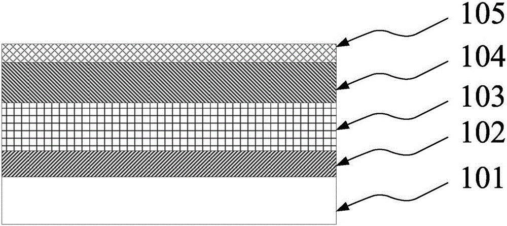
[0037] S1: providing a growth substrate 101, and forming an epitaxial layer on the upper surface of the growth substrate 101;

[0038] S2: forming a metal electrode layer 106 on the surface of the epitaxial layer;

[0039] S3: Perform annealing treatment on the growth substrate 101, the epitaxial layer and the metal electrode layer 106 to enhance the adhesion between the metal electrode layer 106 and the epitaxial layer, and reduce or eliminate the connection between the metal electrode layer 106 and the epitaxial layer. internal stress;

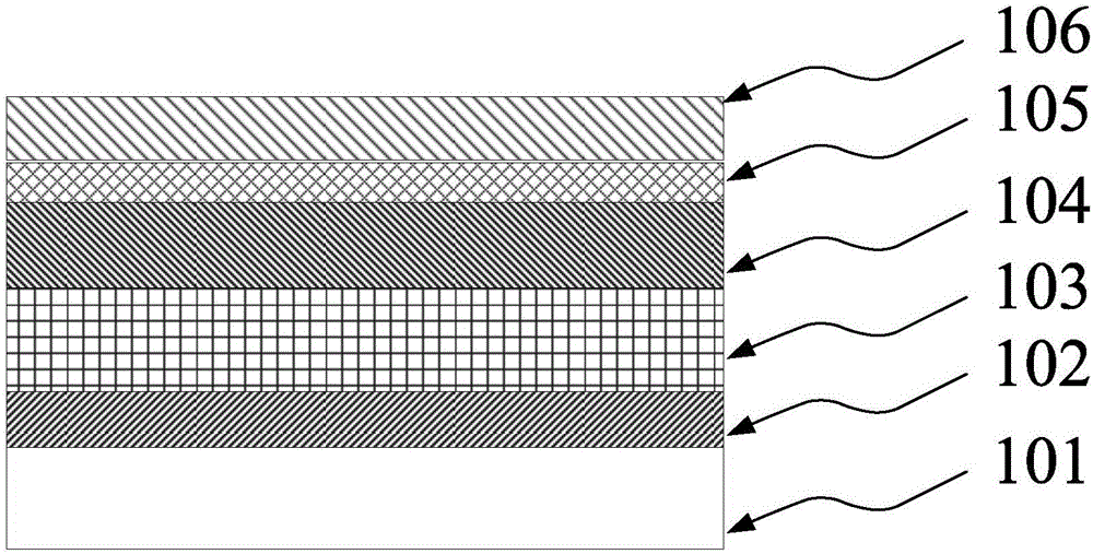
[0040] S4: forming a bonding substrate 107 on the annealed metal electrode layer 106 .

[0041] In step S1, see figure 1 Step S1 in and figure 2 , providing a growth substrate 101 , and forming an epitaxial layer on the growth substrate 101 . Wherein, the epitaxial layer includes an undop...

Embodiment 2

[0054] The present invention provides a vertical LED chip structure, please refer to Figure 4 , the vertical LED chip includes: a growth substrate 101; an epitaxial layer located on the growth substrate 101, the epitaxial layer includes an undoped GaN layer 102, an N- GaN layer 103, multi-quantum well layer 104, and P-GaN layer 105; a metal electrode layer 106 located on the epitaxial layer, the metal electrode layer 106 comprising patterned layers sequentially formed on the P-GaN layer 105 A current spreading layer, a patterned reflective layer and a metal bonding layer, wherein the metal bonding layer is in contact with the epitaxial layer through the patterned current spreading layer and the reflective layer; the bond on the metal electrode layer 106 shown Composite substrate 107. In other embodiments, an N electrode may also be included. The vertical LED chip structure in this embodiment can be obtained by using the preparation method in Embodiment 1.

[0055] Specific...


PUM


Abstract

The invention provides a vertical light emitting diode (LED) chip structure and a fabrication method thereof. The fabrication method comprises the following steps of 1) providing a growth substrate, and forming an epitaxial layer on the growth substrate; 2) forming a metal electrode layer on the epitaxial layer; 3) carrying out annealing processing on the growth substrate, the epitaxial layer and the metal electrode layer so as to improve the adhesion between the metal electrode layer and the epitaxial layer and reduce or eliminate the internal stress between the metal electrode layer and the epitaxial layer; and 4) forming a bonding substrate on the annealed metal electrode layer. By the fabrication method, the problems that a bonding substrate is easy to break or seriously deform and microscopic influence is generated on the epitaxial layer structure and the performance to directly cause serious electric leakage and extremely poor finished rate due to large internal stress of a wafer after bonding during vertical fabrication of a large-sized LED chip in the prior art are solved.

Description

technical field [0001] The invention belongs to the field of LED chips, in particular to a vertical LED chip structure and a preparation method thereof. Background technique [0002] As we all know, due to the constraints of non-conductivity and poor thermal conductivity of the sapphire substrate, the traditional front-mount LED chip has inherent defects such as uneven current distribution and poor heat dissipation. In order to overcome these shortcomings of the front-mount LED chip, the industry is actively developing a vertical-structure LED chip (hereinafter referred to as V-LED). V-LED adopts Si or metal substrate with high conductivity and good heat dissipation. The substrate has good heat conduction, the heat dissipation problem of PN junction is solved, and large-size power chips can be realized. [0003] GaN-based vertical structure LED is a research hotspot of light-emitting semiconductor devices. After years of development, the relatively mature preparation techno...

Claims


Application Information

Patent Timeline
IPC IPC(8): H01L33/36H01L33/00H01L21/60
CPCH01L24/03H01L33/0095H01L33/36H01L2224/03848H01L2933/0016
Inventor 吕孟岩徐慧文李起鸣
Owner ENRAYTEK OPTOELECTRONICS
Why Eureka
Try Eureka