Liquid crystal display panel and liquid crystal display device

A technology of liquid crystal display panels and liquid crystal molecules, which is applied in nonlinear optics, instruments, optics, etc., can solve problems such as serious color mixing at large viewing angles, lower aperture ratio and transmittance of display panels, and limitations in width and spacing process, and achieve Alleviate the effect of color mixing at large viewing angles

Active Publication Date: 2016-07-13
XIAMEN TIANMA MICRO ELECTRONICS +1
View PDF7 Cites 11 Cited by
  • Summary
  • Abstract
  • Description
  • Claims
  • Application Information

AI Technical Summary

Problems solved by technology

[0005] 2) As liquid crystal display panels tend to be more and more high-resolution, the size of the pixel area 130 is getting smaller and smaller, and the width and spacing of the pixel electrodes 111 in the pixel area are limited due to the process;
[0006] 3) For a high-resolution liquid crystal display panel, due to the limitation of the manufacturing process of the array substrate 110 and the color filter substrate 120, in the case of a large viewing angle, the ratio S1 / S of the color shift area to the normal display area gradually increases, and the color mixing at a large viewing angle more serious;
[0007] 4) For a high-resolution liquid crystal display panel, due to the limitation of the manufacturing process of the array substrate 110 and the color filter substrate 120, the aperture ratio and transmittance of the display panel gradually decrease with the increase of the resolution

Method used


Image

  • Liquid crystal display panel and liquid crystal display device
  • Liquid crystal display panel and liquid crystal display device
  • Liquid crystal display panel and liquid crystal display device

Examples


no. 1 example

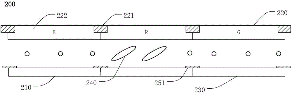
[0034] see first image 3 and Figure 4 , image 3 A cross-sectional view showing a liquid crystal display panel 200 according to a first embodiment of the present invention, Figure 4 A schematic diagram showing a pixel region of the liquid crystal display panel 200 according to the first embodiment of the present invention.

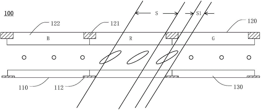
[0035] The liquid crystal display panel includes a first substrate 210 , a second substrate 220 opposite to the first substrate 210 , liquid crystal molecules 240 , a black matrix 221 and a first electrode layer.

[0036] The first substrate 210 is optionally an array substrate. In some embodiments, gate lines, data lines, and thin film transistors are formed on the array substrate 210 . Wherein, a plurality of gate lines and a plurality of data lines are arranged orthogonally, and thin film transistors are used for switch control. The area surrounded by the plurality of gate lines and the plurality of data lines defines the pixel area. The first ...

no. 2 example

[0055] see Figure 5 , Figure 5 A schematic diagram of a pixel area of ​​a liquid crystal display panel according to the second embodiment of the present invention is shown. Figure 5 shown in pixel area 230 with Figure 4 The pixel area 230 shown is similar to the Figure 4 The illustrated pixel area 230 differs in that Figure 5 Among them, the liquid crystal molecules 240' are positive liquid crystal molecules, and the initial alignment direction of the positive liquid crystal molecules 240' is parallel to the X direction. The extension direction of the first branch electrodes 251 is perpendicular to the initial alignment direction of the liquid crystal molecules 240'. That is to say, the extension direction of the first branch electrodes 251 is parallel to the Y direction.

no. 3 example

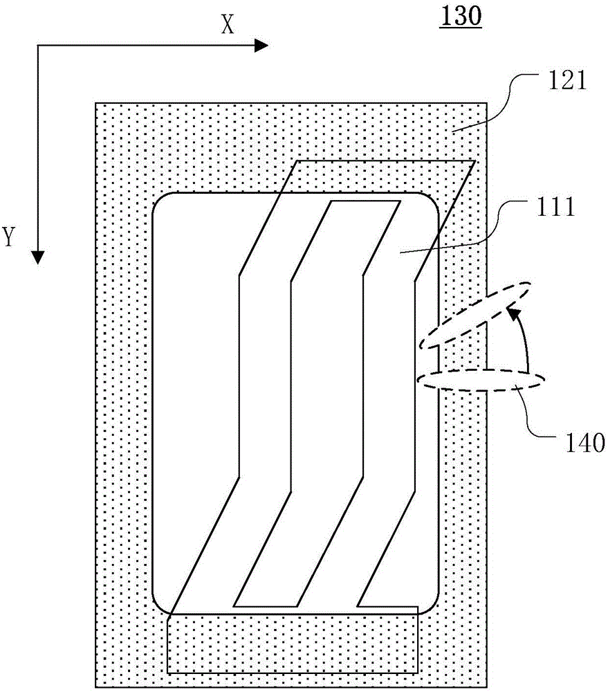
[0057] see Figure 6 , Figure 6 A schematic diagram showing a plurality of pixel regions of a liquid crystal display panel according to a third embodiment of the present invention. exist Figure 6 In the illustrated embodiment, in the plurality of pixel regions 230, each first electrode 250 has a Figure 4 The first electrode 250 shown has the same structure. In each first electrode 250 , a plurality of second branch electrodes 252 are arranged along the Y direction, and the extending direction Z of the plurality of second branch electrodes 252 is the same.


PUM

PropertyMeasurementUnit
widthaaaaaaaaaa
widthaaaaaaaaaa

Abstract

The invention provides a liquid crystal display panel and a liquid crystal display device comprising the same.The liquid crystal display panel comprises a first substrate, a second substrate, liquid crystal molecules, a black matrix and a first electrode layer, wherein the first substrate comprises a plurality of pixel areas, the second substrate is opposite to the first substrate, the liquid crystal molecules are located between the first substrate and the second substrate and has an initial orientation direction, the black matrix is arranged on the second substrate and provided with openings corresponding to all the pixel areas, the first electrode layer is arranged on the first substrate and comprises first electrodes arranged in the pixel areas, and each first electrode comprises a first branch electrode shielded by the black matrix and a plurality of second branch electrodes connected with the first branch electrode, wherein the initial orientation direction of the liquid crystal molecules is set according to the extension direction of the first branch electrodes so that the liquid crystal molecules corresponding to the first branch electrodes can basically not deflect, and angles are formed between the extension direction of the second branch electrodes and the extension direction of the first branch electrodes.By means of the liquid crystal display panel and the liquid crystal display device, the display effect is improved.

Description

technical field [0001] The invention relates to the field of display technology, in particular to a liquid crystal display panel and a liquid crystal display device. Background technique [0002] Liquid crystal display technology mainly realizes the display of images through the deflection of liquid crystal molecules in an electric field. Combine below figure 1 and figure 2 The structure of a liquid crystal display panel in the prior art is described. In the prior art, the liquid crystal display panel 100 includes an array substrate 110 , a color filter substrate 120 opposite to the array substrate 110 , and liquid crystal molecules 140 located between the array substrate 110 and the color filter substrate 120 . The array substrate 110 is divided into a plurality of pixel regions 130 by data lines 112 and gate lines (not shown). The liquid crystal molecules 140 are deflected according to the electric field between the pixel electrode 111 and the common electrode (not sh...

Claims


Application Information

Patent Timeline
Patent Type & Authority Applications(China)
IPC IPC(8): G02F1/1343G02F1/1337
CPCG02F1/133707G02F1/134309
Inventor 马扬昭吴玲
Owner XIAMEN TIANMA MICRO ELECTRONICS
Why Eureka
Try Eureka