
Flash memory and production method thereof

A technology of flash memory and manufacturing method, applied in semiconductor/solid-state device manufacturing, electrical solid-state devices, semiconductor devices, etc., can solve the problems of shortening the channel length, affecting the electrical performance of memory cells, etc., to increase the integration of components and reduce the size. , the effect of shortening the time

Active Publication Date: 2016-07-13
POWERCHIP SEMICON MFG CORP
View PDF4 Cites 1 Cited by
  • Summary
  • Abstract
  • Description
  • Claims
  • Application Information

AI Technical Summary

Problems solved by technology

However, the shortening of the gate length will shorten the channel length (ChannelLength) under the tunnel oxide layer, so when programming this memory cell, abnormal electrical penetration (PunchThrough) will easily occur between the drain region and the source region. ), which will seriously affect the electrical performance of the memory cell

Method used


Image

  • Flash memory and production method thereof
  • Flash memory and production method thereof
  • Flash memory and production method thereof

Examples


Embodiment Construction

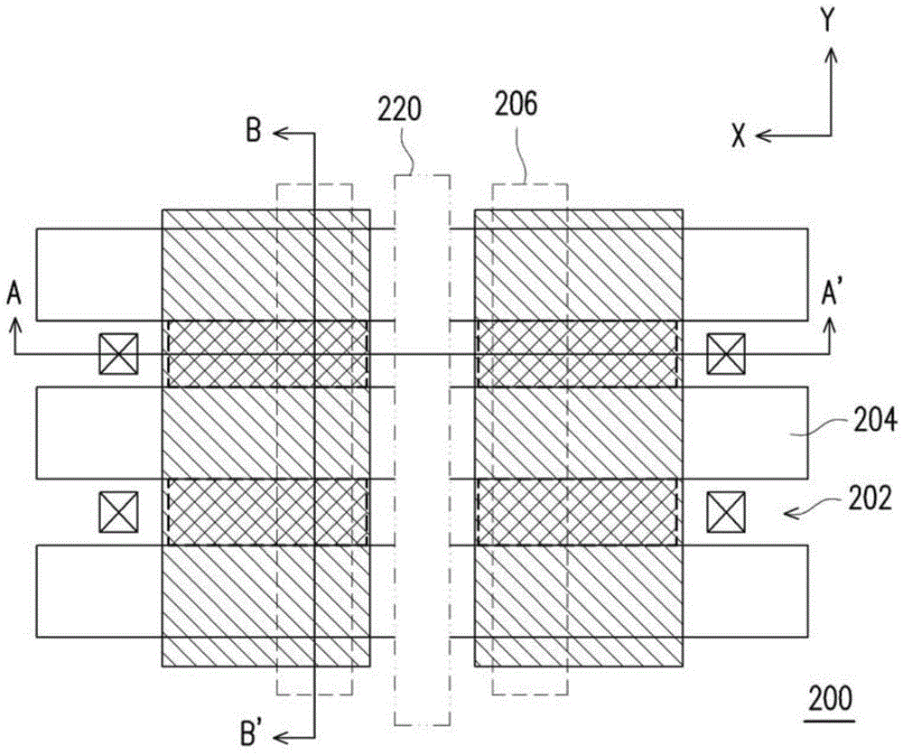
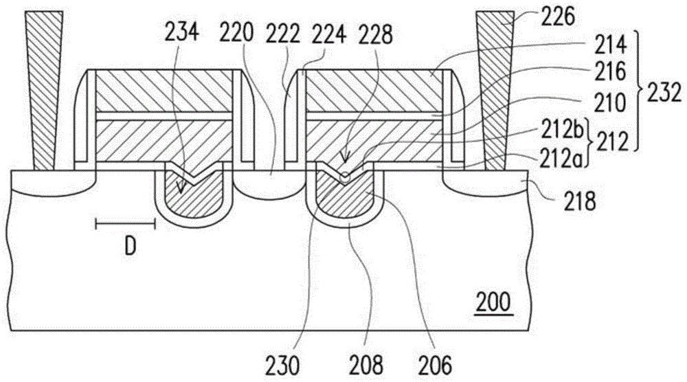
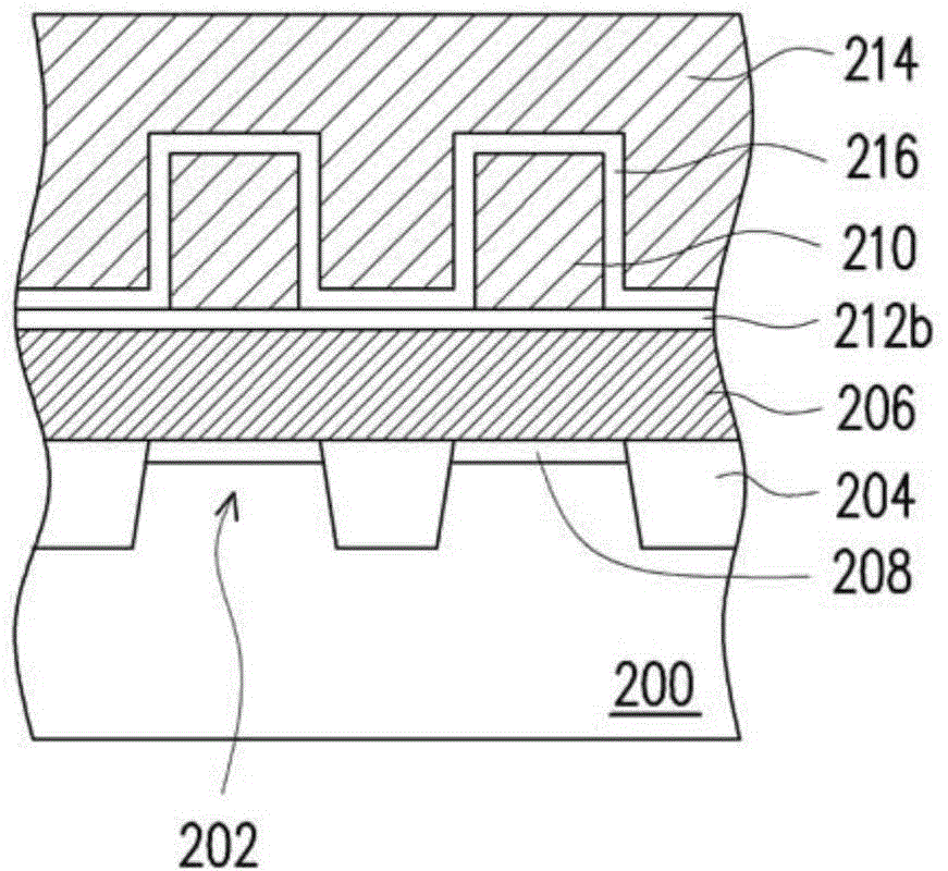
[0059] Figure 1A Shown is a top view of a flash memory according to an embodiment of the present invention. Figure 1B Illustrated as an embodiment of the invention Figure 1A A cross-sectional view of the flash memory in A-A' line. Figure 1C Illustrated as an embodiment of the invention Figure 1A A cross-sectional view along the line B-B' of the flash memory in .

[0060] First, please refer to Figure 1A to Figure 1C , to illustrate the flash memory of the present invention. The flash memory of the present invention includes: a substrate 200, an active region 202, an element isolation structure 204, a selection gate 206, a gate dielectric layer 208, a floating gate 210, a tunneling dielectric layer 212, a control gate 214, a gate Inter-dielectric layer 216, doped region 218 (drain region) and doped region 220 (source region). Wherein, the tunnel dielectric layer 212 , the floating gate 210 , the inter-gate dielectric layer 216 , and the control gate 214 form a stacked ...


PUM


Abstract

The invention discloses a flash memory and a production method thereof. The flash memory comprises a stacked gate structure, a first doped area, a second doped area, a selective gate, and a gate dielectric layer. The stacked gate structure is disposed on a substrate, and the stacked gate structure comprises, from the substrate, sequentially a tunneling dielectric layer, a floating gate, an inter-gate dielectric layer, and a control gate. The first doped area and the second doped area are respectively disposed in the substrate on two sides of the stacked gate structure. The selective gate is disposed in the groove of the substrate under the stacked gate structure, and the selective gate is disposed next to the first doped area, and the distance is arranged between the selective gate and the second doped area. The gate dielectric layer is disposed between the selective gate and the substrate. The tunneling dielectric layer is disposed between the floating gate and the selective gate, and between the floating gate and the substrate.

Description

technical field [0001] The present invention relates to a semiconductor element, and in particular to a flash memory and a manufacturing method thereof. Background technique [0002] Flash memory components have the advantages of being able to store, read, and erase data multiple times, and the stored data will not disappear after power failure, so it has become widely used in personal computers and electronic devices. A non-volatile memory element. [0003] A typical flash memory device uses doped polysilicon to make a floating gate (FloatingGate) and a control gate (ControlGate). Moreover, the floating gate is separated from the control gate by a dielectric layer, and the floating gate is separated from the substrate by a tunnel oxide layer (TunnelOxide). When writing / erasing (Write / Erase) data to the flash memory, by applying a bias voltage to the control gate and the source / drain region, electrons are injected into the floating gate or electrons are released from the f...

Claims


Application Information

Patent Timeline
IPC IPC(8): H01L27/115H01L21/8247H01L27/11524
Inventor 宋达黄明山
Owner POWERCHIP SEMICON MFG CORP
Learn More