
Phase-shifting mask and semiconductor device

Inactive Publication Date: 2005-03-10
BELL SEMICON LLC
View PDF4 Cites 5 Cited by
  • Summary
  • Abstract
  • Description
  • Claims
  • Application Information

AI Technical Summary

Benefits of technology

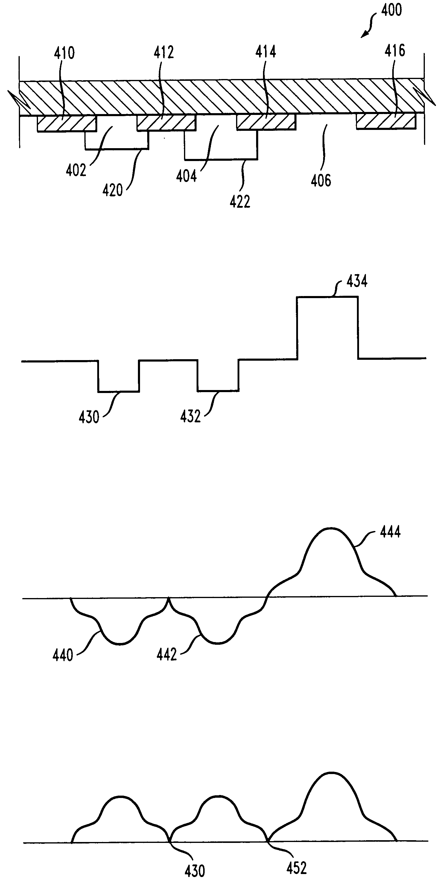
[0014] The invention relates to a phase-shifting mask having substantially equally spaced phases thereby substantially eliminating zeroth order and reducing first order diffraction frequencies. One embodiment of the invention relates to a three-phase-shifting mask having a pattern composed of substantially transparent regions and substantially opaque regions wherein the mask pattern phase-shifts incident radiation by 0, 2 / 3 π and 4 / 3 π radians. The invention further relates to a semiconductor device fabricated utilizing the phase-shifting mask. In such applications the invention facilitates reduction in component size and improved device reliability.

Problems solved by technology

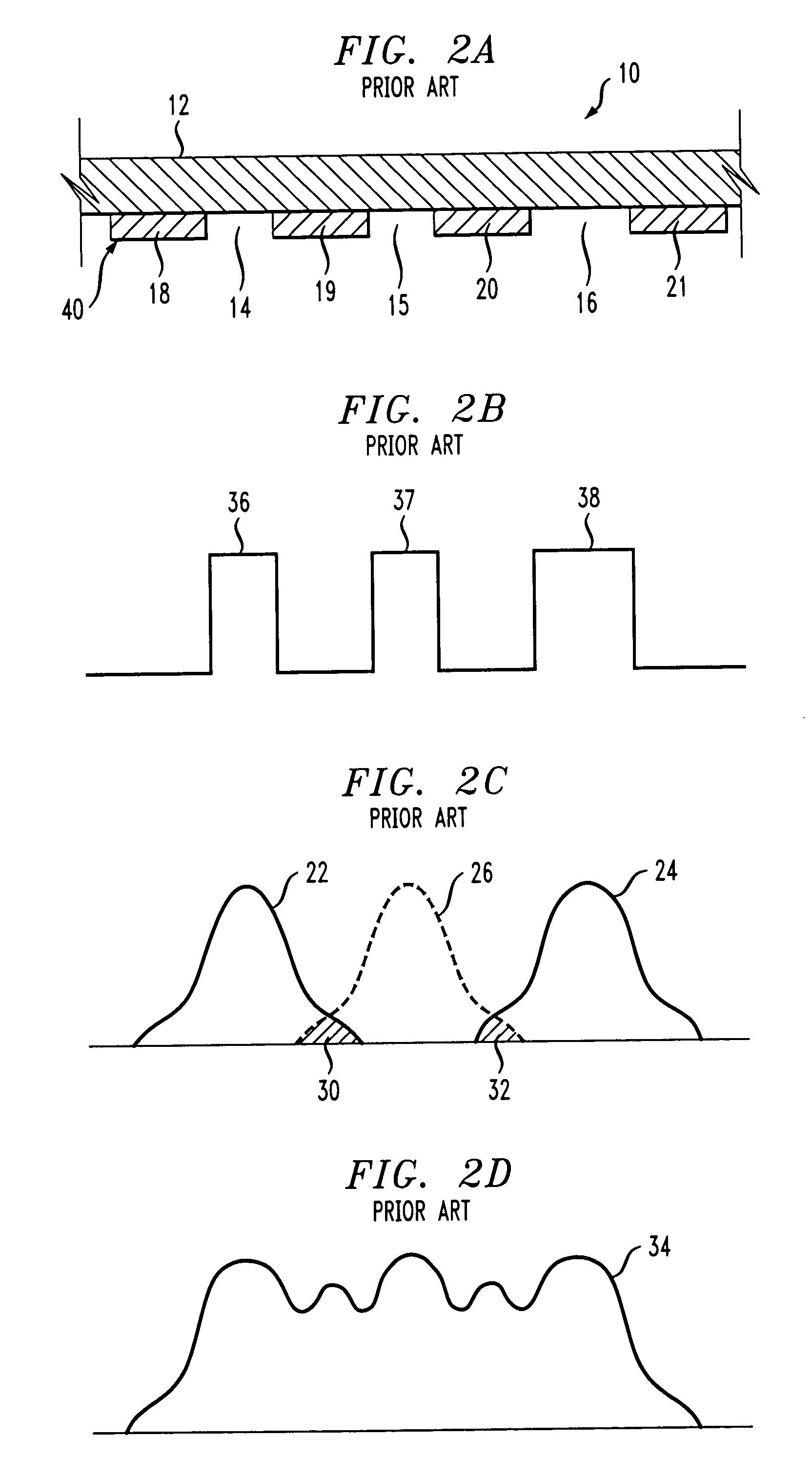
Under this analysis diffraction effects are likely to be produced, decreasing the image resolution even at distance L2, thereby reducing resolution of component features.
As component size decreases, diffraction effects become more significant, thereby limiting reduction in component size.
Decreased sharpness of mask images caused by diffraction effects may reduce product yield and increase device failure rate.
Therefore, even though the electric fields are separated from one another at mask level they may interfere with one another a distance away from the mask, such as at a workpiece surface.
Therefore, there is less contrast in the light intensity distribution at the workpiece surface than at mask level, thereby reducing the resolution capability of the tool.
However, they do not fully resolve all resolution problems, for example a phase conflict may arise for feature configurations in which a phase transmission is generally unavoidable.

Method used


Image

  • Phase-shifting mask and semiconductor device
  • Phase-shifting mask and semiconductor device
  • Phase-shifting mask and semiconductor device

Examples


Embodiment Construction

[0022] It will be appreciated that the following description is intended to refer to specific embodiments of the invention selected for illustration and is not intended to define or limit the invention, other than in the appended claims.

[0023] The invention comprises a phase-shifting mask having substantially equally spaced phases such that the zeroth order diffraction frequency is substantially canceled and the first order diffraction frequency is reduced as compared to nonphase-shifting masks or masks having unequally spaced phases. Any number of equally spaced phases may provide substantially similar pattern transferring results and are within the spirit and scope of the invention. However, the phase-shifting mask preferably has three equally spaced phases to simplify manufacturing. Phase-shifting masks having phase shifts of 1 / 3π radian multiples can be fabricated by layering readily available 1 / 3π radian phase-shifting components.

[0024]FIG. 4A depicts a cross-sectional view o...


PUM

PropertyMeasurementUnit
Thicknessaaaaaaaaaa
Thicknessaaaaaaaaaa
Transparencyaaaaaaaaaa

Abstract

Disclosed is a phase-shifting mask having a pattern comprising a plurality of substantially transparent regions and a plurality of substantially opaque regions wherein the mask pattern phase-shifts at least a portion of incident radiation and wherein the phases are substantially equally spaced, thereby increasing resolution of a given lithographic system. Further disclosed is a semiconductor device fabricated utilizing the phase-shifting mask.

Description

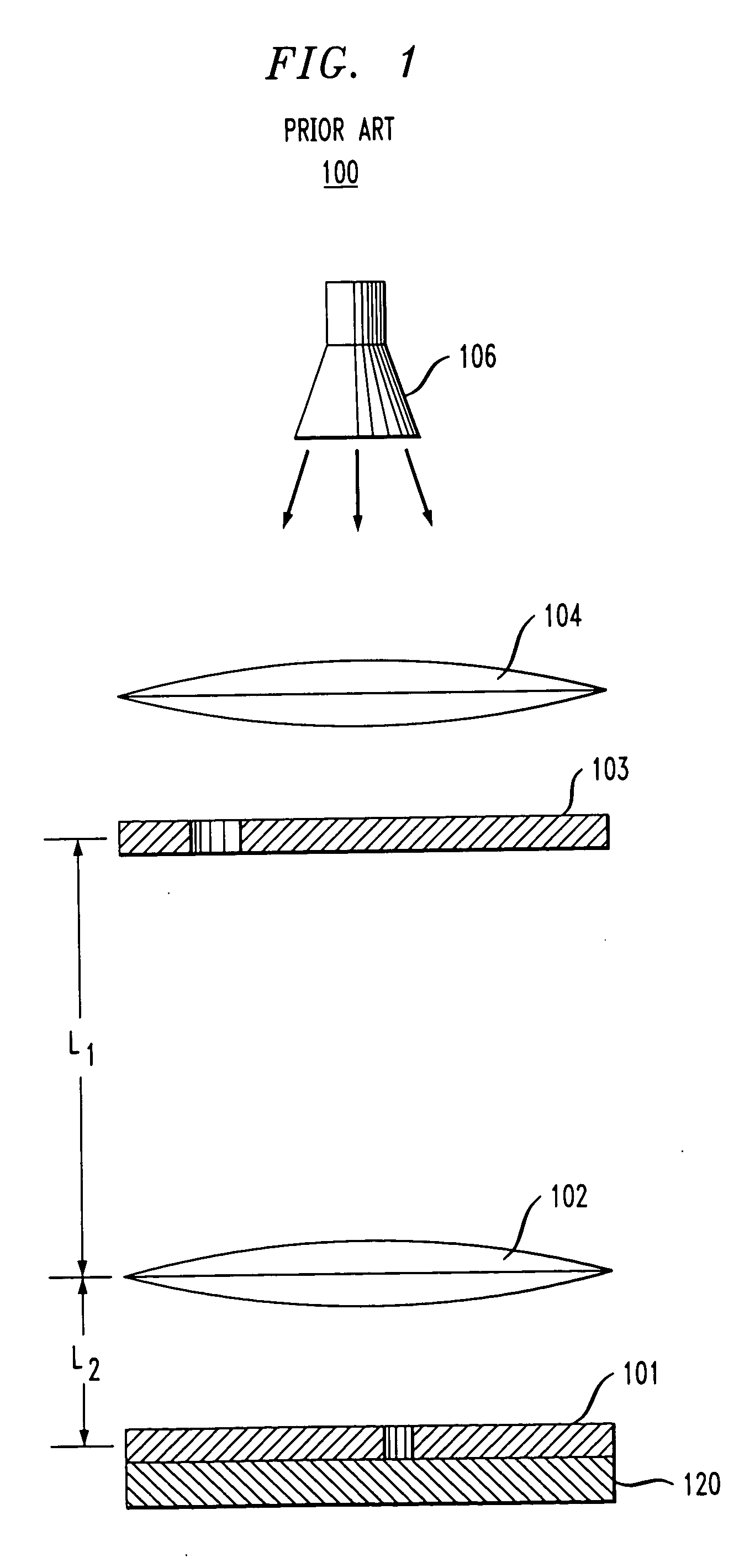
TECHNICAL FIELD OF THE INVENTION [0001] This invention relates to lithographic masks, such as that used for fabricating semiconductor devices. BACKGROUND OF THE INVENTION [0002] Lithography is utilized in semiconductor device manufacturing to pattern features on semiconductor workpiece layers for integrated circuit fabrication. [0003]FIG. 1 shows a lithographic fabrication system 100 for defining features in a workpiece 120, in accordance with prior art. Typically, workpiece 120 comprises a semiconductor substrate, together with one or more layers of substances (not shown) such as silicon dioxide and a resist layer 101, affixed to a surface of workpiece 120. [0004] Typically, radiation of wavelength λ is emitted by an optical source 106, such as a mercury lamp or a laser. The radiation propagates through an optical collimating lens or lens system 104, a patterned lithographic mask 103 having a pattern of opaque and transparent features, and an optical projection lens or lens system ...

Claims


Application Information

Patent Timeline
IPC IPC(8): B31D5/00B65B9/02B65B9/13
CPCB29C66/81812B29C66/4312B31D5/0073B31D2205/0082B29C66/83511B29C65/18B29C66/81811B29C66/133Y10T156/1737B29C66/91421Y10T428/24661B31D2205/0047B29C66/8167B29C66/83423B29C65/305B29C66/0042B29C66/439B29C66/8432B29C65/743B29C66/244B29C66/8161B31D2205/0035B29C66/00441B29C66/8122Y10T428/24562B29C66/1122Y10T156/1025B31D5/0078B29C66/81427B29C66/0342B29K2827/18B29C66/71B29K2023/065
Inventor JIN, FENG
Owner BELL SEMICON LLC
Learn More