
Radio frequency power amplifier circuit
A technology for power amplifiers and amplifier circuits, applied in power amplifiers, high-frequency amplifiers, improving amplifiers to improve efficiency, etc., can solve the problems of low bias current, amplitude and phase distortion that cannot be ignored, etc.
- Summary
- Abstract
- Description
- Claims
- Application Information
AI Technical Summary
Problems solved by technology
Method used
Image

Examples
Embodiment Construction
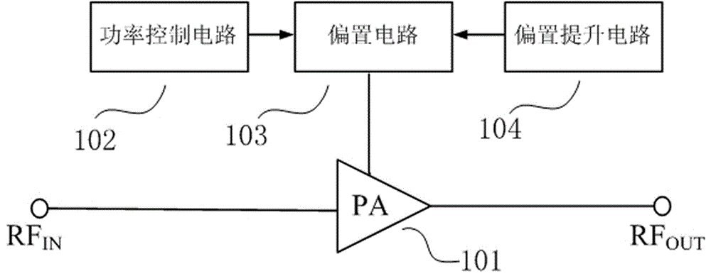
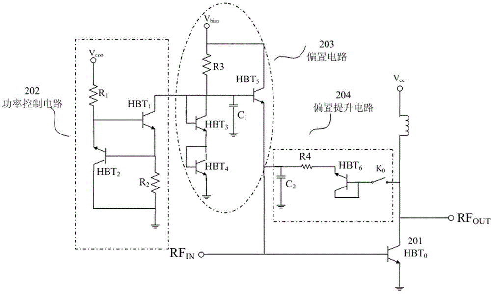
[0015] As shown in the figure, the present invention includes a power amplifier, a power control circuit, a linearization bias circuit and a bias boosting circuit. Output port, NPN transistor HBT 0 connected to the base of the HBT 0 The emitter is grounded, the HBT 0 The collector of the power amplifier is connected to the output port of the power amplifier, the input port of the bias boosting circuit, and one end of the inductor, and the other end of the inductor is connected to the power supply Vcc; the input port of the linearization bias circuit is connected to the output port of the power control circuit.
[0016] The power control circuit is composed of resistor R1, resistor R2, NPN triode HBT 1 and NPN transistor HBT 2 Composition, one end of R1 is connected to the power supply Vcon, and the other end of R1 is respectively connected to HBT 1 Base, HBT 2 connected to the emitter of the HBT 1 The collector is connected to the input port of the linearization bias cir...
PUM
 Abstract
Description
Claims
Application Information