High electron mobility transistor and method of manufacturing the same

a high-electromagnetic transistor and electron mobility technology, applied in the direction of basic electric elements, electrical apparatus, semiconductor devices, etc., can solve the problems of linearity deterioration, distortion, and sometimes kink phenomenon in drain-current/voltage characteristics, and achieve the effect of high electron mobility and preventing kink phenomenon

Inactive Publication Date: 2005-06-21
KK TOSHIBA
View PDF19 Cites 13 Cited by
  • Summary
  • Abstract
  • Description
  • Claims
  • Application Information

AI Technical Summary

Benefits of technology

[0011]An object of the present invention is to provide a compound-semiconduct

Problems solved by technology

However, a conventional GaN-based HEMT has a problem in that a kink phenomenon sometimes occurs in the drain-current/voltage characteri

Method used


Image

  • High electron mobility transistor and method of manufacturing the same
  • High electron mobility transistor and method of manufacturing the same
  • High electron mobility transistor and method of manufacturing the same

Examples


first embodiment

[0044](First Embodiment)

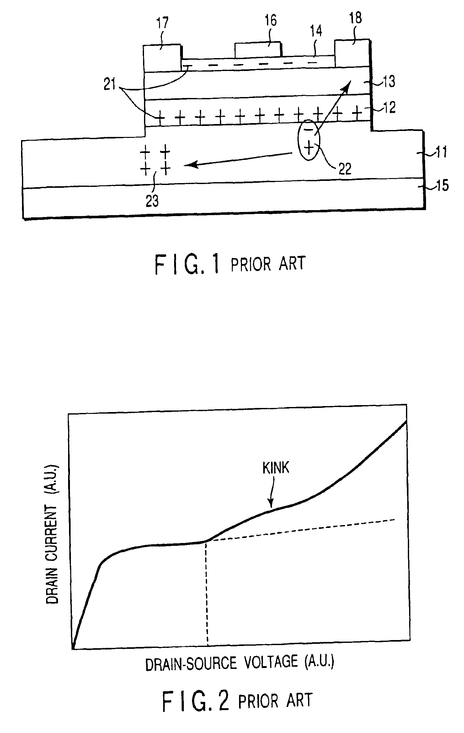
[0045]FIG. 4 is a schematic cross-sectional view of a high electron mobility transistor (HEMT) according to a first embodiment of the present invention. Reference numerals 11, 12, 13, 14 and 15 denote a GaN electron accumulation layer, Alx Ga(1-x)N spacer layer, n-type AlxGa(1-x)N electron supply layer, AlxGa(1-x)N cap layer, and sapphire substrate, respectively. A gate electrode 16 is formed on the cap layer 14, while a source electrode 17 and a drain electrode 18 are formed on the electron supply layer 13. Furthermore, a hole absorption electrode 19 is formed for absorbing holes in a recess portion 24. The recess portion 24 is formed for isolation by removing a peripheral portion, other than an element region, of layers 12, 13 and 14 to reach the electron accumulation layer 11.

[0046]A manufacturing method of the HEMT of the first embodiment is described below. The undoped GaN electron accumulation layer 11 of 2 μm thick is grown on the (0001) sapphire subst...

second embodiment

[0054](Second Embodiment)

[0055]FIG. 5 is a schematic cross-sectional view of a high electron mobility transistor according to a second embodiment of the present invention. The feature of the second embodiment resides in that a p-type semiconductor layer 20 (e.g., p-type GaN layer), or a semiconductor layer having a smaller bandgap width than that of the electron accumulation layer 11 is formed on the undoped GaN electron accumulation layer 11, and thereafter, a hole absorption electrode 19 is formed on the semiconductor layer 20. In this manner, it is possible to absorb holes more effectively than in the first embodiment. In FIG. 5, like reference numerals are used to designate like structural elements corresponding to those in FIG. 4 (the first example) and any further explanation is omitted for brevity's sake.

third embodiment

[0056](Third Embodiment)

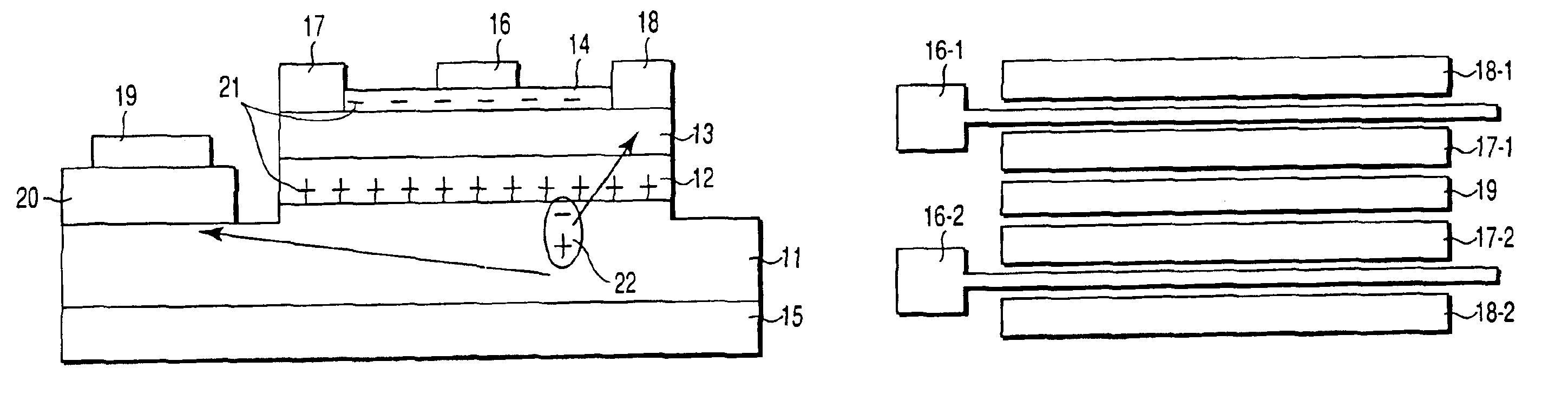
[0057]FIG. 6 is a schematic top view of a high electron mobility transistor according to a third embodiment of the present invention. The first HEMT electrodes are formed of a gate electrode 16-1, a source electrode 17-1, and a drain electrode 18-1. The second HEMT electrodes are formed of a gate electrode 16-2, a source electrode 17-2, and a drain electrode 18-2. The feature of the third embodiment resides in that the hole absorption electrode 19 is formed in parallel with the gate electrode 16-1 in the gate width direction and has substantially the same length as the source electrode 17-1 in the gate width direction. Since the length of the hole absorption electrode 19 is the same as that of the source electrode 17-1, the effect of the hole absorption can be made uniform at any cross section of the drain current direction within the FET, and the kink phenomenon is most effectively suppressed compared to the case where the hole absorption electrode is shorte...


PUM


Abstract

A high electron mobility transistor comprises a GaN-based electron accumulation layer formed on a substrate, an electron supply layer formed on the electron accumulation layer, a source electrode and a drain electrode formed on the electron supply layer and spaced from each other, a gate electrode formed on the electron supply layer between the source and drain electrodes, and a hole absorption electrode formed on the electron accumulation layer so as to be substantially spaced from the electron supply layer. Since the hole absorption electrode is formed on the electron absorption layer in order to prevent holes generated by impact ionization from being accumulated on the electron accumulation layer, a kink phenomenon is prevented. Good drain-current/voltage characteristics are therefore obtained. A high power/high electron mobility transistor is provided with a high power-added efficiency and good linearity.

Description

CROSS-REFERENCE TO RELATED APPLICATIONS[0001]This application is based upon and claims the benefit of priority under 37 CFR §119 from the prior Japanese Patent Applications No. 2000-094574, filed Mar. 30, 2000; and under 37 CFR §120 from U.S. application Ser. No. 10 / 375.084, filed Feb. 28, 2003 now U.S. Pat. No. 6,689,652, which is a divisional application of 09 / 778,823 now U.S. Pat. No. 6,555,851, which issued Apr. 29, 2003, entire contents of which are incorporated herein by reference.BACKGROUND OF THE INVENTION[0002]The present invention relates to a high electron mobility transistor (HEMT), more particularly to a GaN-based HEMT.[0003]It is strongly expected that a nitrogen-compound field-effect transistor using GaN serves as a power element to be operated at a high power and at a high frequency. The nitrogen-compound field-effect transistors which have been proposed are a Schottky gate field-effect transistor, MESFET (metal semiconductor field-effect transistor), HEMT or MODFET ...

Claims


Application Information

Patent Timeline
IPC IPC(8): H01L21/335H01L29/812H01L21/338H01L29/20H01L29/778
CPCH01L29/2003H01L29/7787H01L21/18
Inventor MORIZUKA, MAYUMI
Owner KK TOSHIBA
Why Eureka
Try Eureka