Photoelectric component transfer method

A technology for optoelectronic components and transfer methods, which is applied to electrical components, electrical solid-state devices, circuits, etc., and can solve the problems of different lattice constants of the light-emitting layer, low conversion efficiency of color transfer materials, coating uniformity, and difficulty in growth.

Active Publication Date: 2019-05-03
IND TECH RES INST
View PDF5 Cites 0 Cited by
  • Summary
  • Abstract
  • Description
  • Claims
  • Application Information

AI Technical Summary

Problems solved by technology

However, due to the different lattice constants of the light-emitting layers that can emit different colors of light, it is not easy to grow on the same substrate.
In addition, other existing technologies have proposed a colorization technology using light-emitting diode chips with different color conversion materials, but this technology still faces problems such as low conversion efficiency of color conversion materials and uniformity of coating.

Method used


Image

  • Photoelectric component transfer method
  • Photoelectric component transfer method
  • Photoelectric component transfer method

Examples


no. 1 example

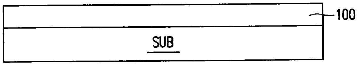
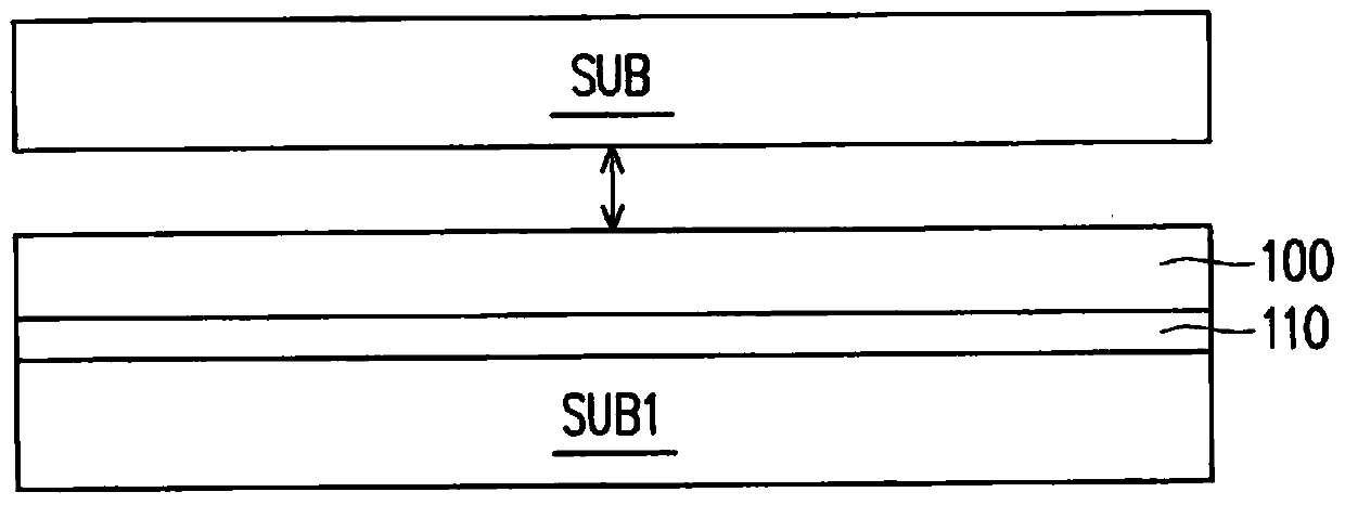
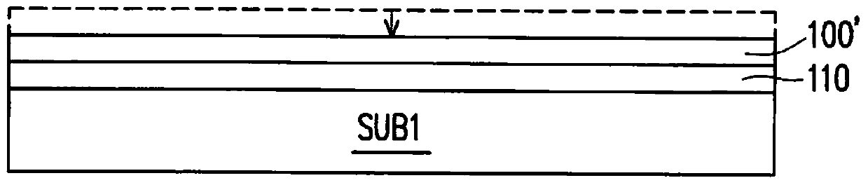
[0034] Figure 1A to Figure 1L It is a schematic flow chart of the photoelectric element transfer method according to the first embodiment of the present invention.

[0035] Please refer to Figure 1A to Figure 1E , firstly, a plurality of photoelectric elements PD arranged in an array are formed on a first substrate SUB1, wherein a sacrificial pattern SC is respectively formed on each photoelectric element PD, such as Figure 1E shown. In this embodiment, the plurality of photoelectric elements PD formed on the same first substrate SUB1 are, for example, light-emitting diode chips (LEDchips) capable of emitting the same color light or photo-sensing chips (photo-sensing chips) with the same photosensitive characteristics. ). For example, the photoelectric element PD can be a red LED chip, a green LED chip, a blue LED chip or a light sensing chip suitable for sensing a specific wavelength. In addition, electrodes (not shown) have been formed on each photoelectric element PD....

no. 2 example

[0054] Figure 2A to Figure 2I It is a schematic flow chart of the photoelectric element transfer method according to the second embodiment of the present invention.

[0055] Please refer to Figure 2A to Figure 2E A plurality of photoelectric elements PD arranged in an array are formed on the first substrate SUB1, wherein a first sacrificial pattern SC1 is respectively formed on each photoelectric element PD. Due to the formation method of the photoelectric element PD and the first sacrificial pattern SC1 and Figure 1A to Figure 1E , Figure 1E 'as well as Figure 1E " is similar, so it will not be repeated here. It should be noted that in this embodiment, the fabrication of the first sacrificial pattern SC1 can be omitted. In other words, the fabrication of the first sacrificial pattern SC1 is not necessary.

[0056] Then please refer to Figure 2F , forming a magnetic material layer M on the first sacrificial pattern SC1, so that the photoelectric element PD is covere...

no. 3 example

[0064] Figure 3A to Figure 3I It is a schematic flow chart of the photoelectric element transfer method according to the first embodiment of the present invention.

[0065] Please refer to Figure 3A to Figure 3E First, a plurality of photoelectric elements PD arranged in an array are formed on a first substrate SUB1, wherein a first sacrificial pattern SC1 and a second sacrificial pattern SC2 are respectively formed on each photoelectric element PD, and the first sacrificial pattern SC1 covers the photoelectric elements PD. On the element PD, and the second sacrificial pattern SC2 is located between the photoelectric element PD and the first substrate, and the photoelectric element PD is sandwiched between the first sacrificial pattern SC1 and the second sacrificial pattern SC2, as Figure 3E shown. In this embodiment, the plurality of photoelectric elements PD formed on the same first substrate SUB1 are, for example, light-emitting diode chips (LEDchips) capable of emitti...


PUM


Abstract

A transfer-bonding process for photoelectric devices comprising: providing a first substrate having a plurality of photoelectric devices formed thereon, the photoelectric devices being arranged in an array; selectively forming a magnetic material layer on partial photoelectric devices so as to cover the partial photoelectric devices by magnetic materials; utilizing a magnetic suction end to absorb the magnetic material layer so as to separate the photoelectric devices covered by the magnetic materials from a first substrate, and allow the photoelectric devices to absorb the magnetic suction end; and transferring the photoelectric devices by the magnetic materials to a second substrate.

Description

technical field [0001] The invention relates to a method for manufacturing a photoelectric element, and in particular to a method for transferring a photoelectric element. Background technique [0002] Inorganic light-emitting diode displays have the characteristics of active light emission and high brightness, so they have been widely used in lighting, display and other technical fields. But monolithic micro-displays have always faced the technical bottleneck of colorization. At present, existing technologies propose to use epitaxial technology to fabricate multiple light-emitting layers capable of emitting different colors of light in a single LED chip, so that a single LED chip can provide different colors of light. However, since the lattice constants of the light-emitting layers that can emit different colors of light are different, it is not easy to grow on the same substrate. In addition, other existing technologies have proposed a colorization technology using ligh...

Claims


Application Information

Patent Timeline
Patent Type & Authority Patents(China)
IPC IPC(8): H01L21/78H01L27/15H01L27/144
Inventor 吴明宪方彦翔安超群
Owner IND TECH RES INST
Why Eureka
Try Eureka