Manufacturing method for etch-back printed circuit board

A technology for printed circuit boards and manufacturing methods, which is applied in the fields of printed circuit manufacturing, printed circuits, printed circuits, etc., can solve problems such as difficult removal of glass fibers, unfavorable electrical connection reliability between inner and outer layers, etc., so as to ensure the lamination effect, The effect of stable size and firm connection

Active Publication Date: 2016-07-20
JIANGMEN SUNTAK CIRCUIT TECH
View PDF4 Cites 9 Cited by
  • Summary
  • Abstract
  • Description
  • Claims
  • Application Information

AI Technical Summary

Problems solved by technology

[0003] The present invention aims at the problem that it is difficult to remove the glass fiber at the hole wall in the existing etch-back process for making the etch-out printed circuit board, which is not conducive to better improving the reliability of the electrical connection between the inner and outer layers, and provides a kind of etch-out effect that can be used. Manufacturing method of recessed printed circuit board for better improving electrical connection reliability between inner and outer layers

Method used


Image

  • Manufacturing method for etch-back printed circuit board
  • Manufacturing method for etch-back printed circuit board
  • Manufacturing method for etch-back printed circuit board

Examples


Embodiment

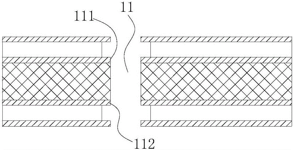
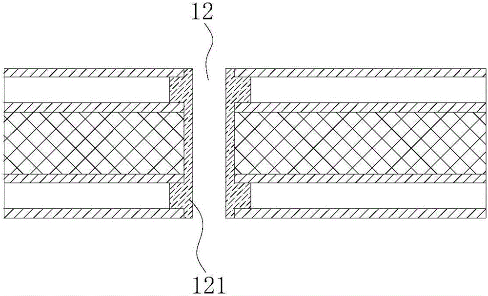
[0021] This embodiment provides a method for manufacturing an etched printed circuit board. The etched printed circuit board includes metallized etch holes, and the metallized etch holes are formed by metallizing the etch holes. The etch-back hole is formed after the through-hole is etched back.

[0022] The specific production steps are as follows:

[0023] (1) Making the inner core board

[0024] First, the base material is cut to obtain a core board of a predetermined size. Then bake the board, that is, place the core board at 150-175° C. to bake the core board for 4 hours. Next, according to the prior art, the inner layer circuit is made on the core board through the negative process to obtain the inner layer core board.

[0025] (2) Drill preset holes

[0026] Drill preset holes on the prepreg, the drilled preset holes correspond to the through holes to be made in the subsequent process and the center of the preset hole overlaps with the center of the through hole; in...


PUM


Abstract

The invention relates to the technical field of circuit board production, particularly to a manufacturing method for an etch-back printed circuit board. According to the invention, preset holes that correspond to through holes one by one and have apertures larger than those of the through holes are drilled in a prepreg and thus pieces of glass fiber cloth corresponding to the through holes needing follow-up etching back processing are removed in advance, and only resin in the holes needs to be removed at a de-smearing step, so that a problem that the glass fiber cloth can not be removed easily can be solved; and a good etch-back effect and a good hole wall effect can be formed and the inner layer circuit cooper can be exposed fully. After through hole metallization, three-dimensional connection is formed between the hole wall copper-plated layer and the inner layer circuit cooper, so that the two parts can be connected firmly and thus reliability of electrical connection between the inner layer and the outer layer can be improved. The apertures of the preset holes are set to be larger than those of the through holes by 0.05 mm; losing of too much resin for the prepreg can be avoided while the glass fiber cloth is removed completely; and the influence on compressing by the resin loss of the prepreg due to hole drilling can be reduced.

Description

technical field [0001] The invention relates to the technical field of printed circuit board production, in particular to a method for manufacturing a recessed printed circuit board. Background technique [0002] Printed circuit board (Printed Circuit Board, PCB) is also called printed circuit board. With the development of technology, higher and higher requirements are put forward for the precision and reliability of printed circuit boards. In order to improve the high reliability of the electrical connection between the inner and outer layers of the (multi-layer) printed circuit board, a certain amount of resin and glass fiber on the hole wall can be removed after drilling to completely expose the inner layer copper at the hole wall After sinking copper and electroplating the whole plate to metallize the hole wall, a three-dimensional connection is formed between the copper plating layer on the hole wall and the inner line copper, which makes the connection between the tw...

Claims


Application Information

Patent Timeline
Patent Type & Authority Applications(China)
IPC IPC(8): H05K3/00H05K3/42
CPCH05K3/0047H05K3/429H05K2201/09563
Inventor 敖四超寻瑞平张义兵钟宇玲
Owner JIANGMEN SUNTAK CIRCUIT TECH
Why Eureka
Try Eureka