Liquid crystal display panel and manufacturing method thereof

A technology for a liquid crystal display panel and a manufacturing method, which is applied in nonlinear optics, instruments, optics, etc., can solve the problems of uneven brightness, uneven cell thickness, easy to fall into, and achieves low production cost, simple and simplified production method. The effect of the process flow

Inactive Publication Date: 2016-07-27
TCL CHINA STAR OPTOELECTRONICS TECH CO LTD
View PDF9 Cites 16 Cited by
  • Summary
  • Abstract
  • Description
  • Claims
  • Application Information

AI Technical Summary

Problems solved by technology

[0003] In the development process of TFT-LCD, large size, high resolution and curved surface are the technological development trend, but with the current design, the PS is designed on the color filter substrate, and the PS is easy to fall into the TFT array substrate during the bending process of the curved liquid crystal panel. At the through hole (Viahole) on the top, the thickness of the box is uneven, resulting in uneven brightness (Mura)

Method used


Image

  • Liquid crystal display panel and manufacturing method thereof
  • Liquid crystal display panel and manufacturing method thereof
  • Liquid crystal display panel and manufacturing method thereof

Examples


Embodiment Construction

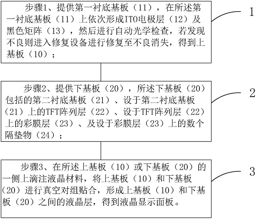
[0027] In order to further illustrate the technical means adopted by the present invention and its effects, the following describes in detail in conjunction with preferred embodiments of the present invention and accompanying drawings.

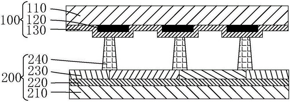
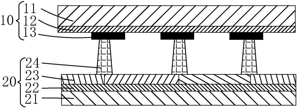
[0028] see figure 2 , the present invention provides a liquid crystal display panel, comprising an upper substrate 1 and a lower substrate 2 arranged oppositely, and a liquid crystal layer (not shown) arranged between the upper substrate 1 and the lower substrate 2;

[0029] The upper substrate 1 includes a first base substrate 11, an ITO electrode layer 12, and a black matrix 13 arranged in sequence facing the liquid crystal layer;

[0030] The lower substrate 2 includes a second base substrate 21 , a TFT array layer 22 , a color filter layer 23 , and several spacers 24 arranged in sequence facing the liquid crystal layer.

[0031] Specifically, the color filter layer 23 includes several color-resist units 231 arranged in an array, the blac...


PUM


Abstract

The invention provides a liquid crystal display panel and a manufacturing method thereof. In the liquid crystal display panel, a COA (Color Filter on Array) and POA (PS on Array) design is adopted, so that the problem of formation of Mura due to a non-uniform box thickness since post spacers tend to fall into through holes on an TFT (Thin Film Transistor) array substrate in a panel bending process is solved. A black matrix of an upper substrate is arranged on an ITO (Indium Tin Oxide) electrode layer, so that a manufacturing method is simple, AOI (Automatic Optic Inspection) equipment and repairing equipment are omitted, and the production cost is low. The manufacturing method of the liquid crystal display panel comprises the following steps: forming the ITO electrode layer of the upper substrate, and forming the black matrix on the ITO electrode layer; performing AOI and repairing processes by using the AOI equipment and the repairing equipment on a yellow line where the black matrix is positioned. The AOI equipment and the repairing equipment under a production line at which the ITO electrode layer is positioned are omitted, the AOI and repairing processes only need to be performed once, the process flow of the upper substrate is simplified, the equipment space is saved, and the purchasing cost is reduced.

Description

technical field [0001] The invention relates to the field of display technology, in particular to a liquid crystal display panel and a manufacturing method thereof. Background technique [0002] Active thin film transistor liquid crystal display (ThinFilmTransistor-LCD, TFT-LCD) has been developed rapidly and widely used in recent years. Most of the liquid crystal display devices currently on the market are backlight liquid crystal display devices, which include a liquid crystal display panel and a backlight module. Usually, the liquid crystal display panel is composed of a color filter (ColorFilter, CF) substrate, a thin film transistor (ThinFilmTransistor, TFT) array substrate, a liquid crystal (LiquidCrystal, LC) sandwiched between the color filter substrate and the TFT array substrate, and a sealant (Sealant). ; Its working principle is to control the rotation of the liquid crystal molecules in the liquid crystal layer by applying a driving voltage on the two glass subs...

Claims


Application Information

Patent Timeline
Patent Type & Authority Applications(China)
IPC IPC(8): G02F1/1335G02F1/1339G02F1/13G02F1/1362
CPCG02F1/1309G02F1/133512G02F1/13394G02F1/1362G02F1/136222
Inventor 阙祥灯
Owner TCL CHINA STAR OPTOELECTRONICS TECH CO LTD
Why Eureka
Try Eureka