

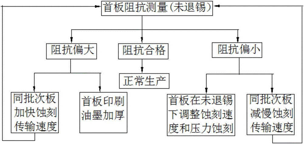
Control method for impedance of outer layer
A control and outer layer technology, applied in the chemical/electrolytic method to remove conductive materials, printed circuit components, electrical components, etc., can solve the problem that the finished product does not meet the requirements, the finished product impedance of the first board exceeds the standard and is scrapped, and there is an open circuit risk And other issues
- Summary
- Abstract
- Description
- Claims
- Application Information
AI Technical Summary
Problems solved by technology
Method used
Image

Examples
example 1
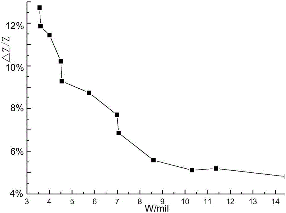
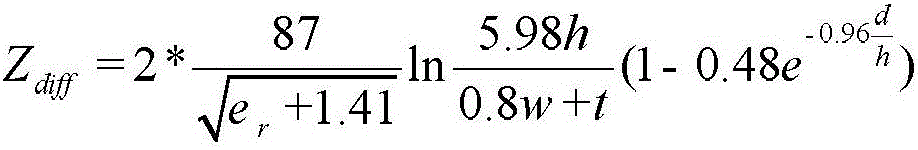
[0065] Example 1: In a factory, the thickness of copper plating on the outer layer is 35um, the thickness of solder resist is 50um, and the thickness of tin plating is 8um on average. 0 and the impedance value after etching (with tin) is Z 1 , the design line width includes a single-ended line of 3.5mil to 14.5mil. According to statistics, the impedance fluctuation range of the two has the following relationship:
[0066] Table 1-1 Effects of single end cap before and after solder mask
[0067]
[0068] In Table 1-1, w is the line width, the unit is mil; Z is the design impedance value, the unit is ohm; wiring layer: shielding layer, indicating the number of layers where the wiring layer is located and the number of layers where the shielding layer is located; Group 1 to Group 8 represents the data of △Z measured for 8 times, the average value is the average value of △Z of the eight groups of data, △Z / Z% is the percentage of △Z of the average value and the design impedance...
example 2
[0071] Table 1-2 Effects of differential cover before and after solder mask
[0072]
[0073] Similar to Example 1, in Table 1-2, w is the line width, in mil; Z is the design impedance value, in ohm, and the first to eighth groups represent the data of △Z measured 8 times, and the average value is eight groups The average value of △Z of the data, △Z / Z% is the percentage of △Z of the average value and the design impedance value Z, △Z / Z% indicates the percentage of impedance change;
[0074] In Example 2: For the control board with 10% impedance tolerance, the area is divided according to the first board control coefficient a=0.3. When the differential line width of the outer layer is 3-4.5mil, the difference between the impedance of the finished product and the impedance of the semi-finished product is △X 1 =△Z 1 / Z is controlled according to 15%; when the line width is 4.5~7mil, the difference between the impedance of the finished product and the impedance of the semi-fin...
PUM
 Abstract
Description
Claims
Application Information