
Eureka
For R&D, Eureka makes reading and utilizing patents & technical documents easy.
Eureka AIR
Designed for self-driven R&D workflows. Generate viable solutions, solve complex R&D challenges, empower your innovation with AI.

Eureka Materials
Designed for material experts only. Revolutionize your material R&D, from search, analyze, to developing new materials.

TechResearch
Generate reliable direction feasibility study reports for your R&D in just a few steps.

TechSeek
Discover and master advanced knowledge NOW. Basics, ideas, possibilities, all at once.

TechMind
As an expert in R&D Theories, TechMind can generates customized viable solutions instantly.

TechRisk
Analyze your overall solution with one click, know your potential R&D risks in advance.

TechMonitor
Get weekly tech updates, stay abreast of the latest tech innovations and key insights.
Voltage distribution method and apparatus for flash memory unit model
A flash memory cell and voltage distribution technology, applied in the field of memory, can solve the problems of low accuracy of flash memory cell model simulation results, etc.
- Summary
- Abstract
- Description
- Claims
- Application Information
AI Technical Summary
Problems solved by technology
Method used
Image

Examples
Embodiment Construction
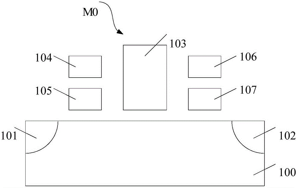
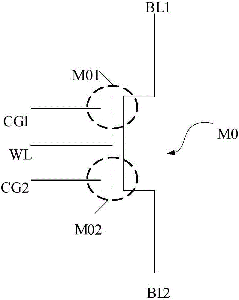
[0085] Below to figure 1 and figure 2 Take the flash memory cell shown as an example, and explain in detail how to distribute the voltage of the flash memory cell model during the use of the existing flash memory cell model:
[0086] figure 1 It is a schematic cross-sectional structure diagram of an existing flash memory unit M0. The flash memory unit M0 has a double split-gate transistor structure and includes two symmetrically distributed storage structures, and each storage structure stores one bit of data. Specifically, the flash memory unit M0 includes: a substrate 100 ; an intermediate electrode 103 located above the substrate 100 ; and a first storage structure and a second storage structure symmetrically distributed on both sides of the intermediate electrode 103 .
[0087] Wherein, the first storage structure includes a first bit line electrode 101, a first control gate 104, and a first floating gate 105; the second storage structure includes a second bit line elec...
PUM
 Abstract
Description
Claims
Application Information
 - R&D Engineer
- R&D Manager
- IP Professional
- Industry Leading Data Capabilities
- Powerful AI technology
- Patent DNA Extraction
Browse by: Latest US Patents, China's latest patents, Technical Efficacy Thesaurus, Application Domain, Technology Topic, Popular Technical Reports.
© 2024 PatSnap. All rights reserved.Legal|Privacy policy|Modern Slavery Act Transparency Statement|Sitemap|About US| Contact US: help@patsnap.com