LED luminescent device and LED light source

A technology for light-emitting devices and LED chips, applied in the direction of electric solid devices, semiconductor devices, electrical components, etc., can solve the problems of affecting the life of LED chips, easy aging, etc., to achieve the effect of firm and reliable structure, change aging, and reduce light loss.

Active Publication Date: 2016-08-10
苏州汇杰紫芯光电有限公司
View PDF7 Cites 3 Cited by
  • Summary
  • Abstract
  • Description
  • Claims
  • Application Information

AI Technical Summary

Problems solved by technology

Moreover, the sealed package between the quartz glass substrate and the lower substrate is generally completed by bonding with an adhesive. Organic materials such as adhesives are easily aged under the action of ultraviolet rays, so that the connection between the substrate and the lower substrate fails and enters directly into moisture, etc. Affect LED chip life

Method used


Image

  • LED luminescent device and LED light source
  • LED luminescent device and LED light source
  • LED luminescent device and LED light source

Examples


Embodiment 1

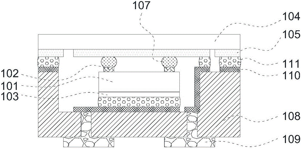
[0047] Such as figure 2 As shown, this embodiment discloses an LED light-emitting device, the LED light-emitting device includes an LED chip 101, an upper substrate 104 and a lower substrate 108, the upper substrate 104 and the lower substrate 108 are fastened to form an LED receiving cavity, and the LED chip 101 surrounded by it. In the figure, the cross-sectional view of the lower substrate is a U-shaped structure, which does not represent a limitation to the present invention. The equivalent structure can also be that the upper substrate is an inverted U-shaped structure, and the lower substrate is a flat plate structure. This simple change is all part of the present invention. protected range.

[0048] Wherein, the LED chip 101 is an ultraviolet LED chip with a vertical structure, and the emission wavelength range of the chip is 240-420nm. The chip N electrode 102 and the chip P electrode 103 are respectively located on the upper and lower sides of the chip. The material...

Embodiment 2

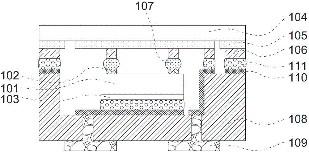
[0055] Such as image 3 As mentioned above, this embodiment also discloses an LED light-emitting device, the main structure of which is the same as that of Embodiment 1, the difference is that in this embodiment, in order to improve the performance of electrical connection, a layer of conductive circuit connection is also provided under the transparent conductive layer 105. Layer 106, the main material of the conductive circuit connection layer 106 is Ti-Au plating.

Embodiment 3

[0057] Such as Figure 4 , Figure 5 , Image 6 As shown, this implementation discloses a schematic structural diagram of four vertically structured LED chips; this embodiment repeatedly sets four identical LED chips on the basis of Embodiment 2.

[0058] Such as Figure 4 As shown, there are four side-by-side LED chips 201 seen through the upper substrate, Figure 5 yes Figure 4 A-axis cross-sectional view, which is the longitudinal cross-sectional view of one of the LED chips, is attached Figure 5 And attached image 3 It can be seen from the comparison that the structures of the two are exactly the same, and different marks are only made in the drawings to distinguish the situation of multiple chips, such as the attached image 3 In the case of a single LED, 101 in the figure represents the LED chip, attached Figure 5 In order to distinguish, the LED chip is identified as 201, for example, 202 indicates the N electrode of the chip, for example, 203 indicates the P...


PUM


Abstract

The present invention discloses a LED luminescent device and a LED light source. The LED luminescent device comprises a LED chip with a vertical structure, an upper substrate and a lower substrate, wherein the upper substrate and the lower substrate are buckled to form a LED holding cavity to enclose the LED chip; the P electrode of the LED chip is led out by the P electrode lead-out circuit arranged at the lower substrate; the N electrode of the LED chip is electrically connected with the N electrode connection layer distributed on the substrate, and the N electrode connection layer is connected with the lower substrate through the leading wire arranged on the LED holding cavity side wall for leading out; and the packaging connection positions of the upper substrate and the lower substrate employ inorganic materials for connection, and the upper substrate is a transparent substrate. The LED luminescent device and the LED light source are longer in service life and smaller in the LED light extraction loss.

Description

technical field [0001] The invention belongs to the technical field of LEDs, and in particular relates to an LED light-emitting device and an LED light source packaged with an all-inorganic material. Background technique [0002] LED has the advantages of small size, low driving voltage, high luminous efficiency, long life, etc., and has been used in many lighting and decoration products. LEDs that can emit ultraviolet light have many applications in the fields of curing, identification, detection, sterilization, and disinfection with the improvement of luminous efficiency. [0003] The packaging of existing high-power ultraviolet LEDs still cannot avoid the use of organic materials. During long-term use, the organic materials will age and deteriorate under ultraviolet light, resulting in poor sealing and poor permeability, which affects the use of the product. [0004] Moreover, the existing vertical structure LED packaging structure, such as figure 1 As shown, the N elec...

Claims


Application Information

Patent Timeline
Patent Type & Authority Applications(China)
IPC IPC(8): H01L33/52H01L33/62
CPCH01L2224/48091H01L2224/48227H01L2224/73253H01L2224/73265H01L2924/00014H01L33/52H01L33/62
Inventor 陈海英李正豪许朝军
Owner 苏州汇杰紫芯光电有限公司
Why Eureka
Try Eureka