Supercharge Your Innovation With Domain-Expert AI Agents!

An array substrate, a method for manufacturing the array substrate and a display device

A technology of an array substrate and a manufacturing method, which is applied in the field of display devices, can solve problems such as reducing the brightness of a display panel, and achieve the effects of reducing energy consumption and improving brightness

Inactive Publication Date: 2016-08-17
BOE TECH GRP CO LTD
View PDF4 Cites 4 Cited by
  • Summary
  • Abstract
  • Description
  • Claims
  • Application Information

AI Technical Summary

Problems solved by technology

Most color filter substrates are realized by setting a filter layer including colored color-resist blocks on the base substrate, which will reduce the brightness of the display panel

Method used


Image

  • An array substrate, a method for manufacturing the array substrate and a display device
  • An array substrate, a method for manufacturing the array substrate and a display device
  • An array substrate, a method for manufacturing the array substrate and a display device

Examples


Embodiment approach

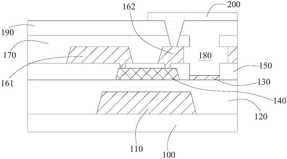
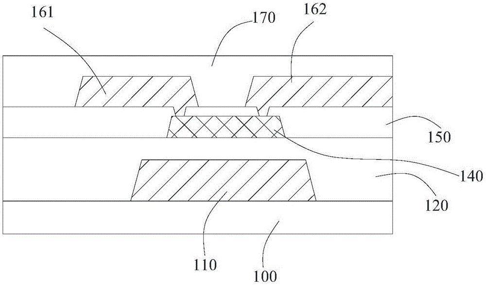
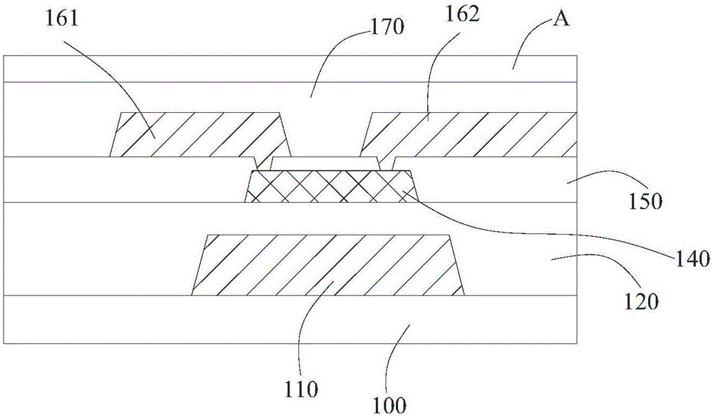
[0070] As a preferred implementation manner, the active layer 140 of the thin film transistor is made of oxide, and the transparent filter layer 150 is located between the active layer 140 of the thin film transistor and the layer where the source electrode 161 is located. As shown in the figure, the source electrode 161 and the drain electrode are respectively connected to the active layer 140 through via holes penetrating through the transparent filter layer 150 . In the present invention, the transparent filter layer 150 can also be used as an etch stop layer to prevent damage to the active layer 140 during the steps of forming the source and drain electrodes. As a preferred embodiment of the present invention, the active layer 140 can be made of IGZO.

[0071] In the present invention, the specific material of the transparent filter layer 150 is not particularly limited, as long as it can allow light to pass through. As a preferred embodiment of the present invention, the...


PUM

PropertyMeasurementUnit
thicknessaaaaaaaaaa
thicknessaaaaaaaaaa
thicknessaaaaaaaaaa

Abstract

The invention provides an array substrate which is divided into a plurality of pixel units. Each pixel unit is inside provided with a light filter structure. Each light filter structure comprises a first shading member and a second shading member arranged in the thickness direction of the array substrate in a spaced manner; the second shading member comprises a second shading member body and a light hole running through the second shading member body in the thickness direction; a light transmitting gap is formed between the inner edge of the orthographic projection, on the layer where the first shading member is located, of the second shading member body and the edge of the first shading member; a transparent light transmitting space is formed above the first shading member; the light transmitting gap enables light passing through the light transmitting gap to have a preset wavelength. The invention also provides a method for manufacturing the array substrate and a display device. When the display device is used for display, color display can be realized and energy consumption can be reduced.

Description

technical field [0001] The present invention relates to the field of display devices, in particular, to an array substrate, a method for manufacturing the array substrate, and a display device including the array substrate. Background technique [0002] For many display panels (for example, liquid crystal display panels), a color filter substrate needs to be provided to realize color display. Most of the color filter substrates are realized by disposing a filter layer including colored color-resist blocks on the base substrate, which will reduce the brightness of the display panel. [0003] Therefore, how to realize color display without affecting the brightness of the display panel has become a technical problem to be solved urgently in this field. Contents of the invention [0004] The object of the present invention is to provide an array substrate, a method for manufacturing the array substrate, and a display device including the array substrate. The display device in...

Claims


Application Information

Patent Timeline
Patent Type & Authority Applications(China)
IPC IPC(8): G02F1/1335H01L21/77
CPCG02F1/133514G02F1/133516H01L27/1259G02F1/1368H01L27/1248G02F1/136222G02F1/136231G02F1/136209G02F1/136227G02F2203/01G02F2203/05G02F2203/15H01L27/1262
Inventor 王东方
Owner BOE TECH GRP CO LTD
Features
  • R&D
  • Intellectual Property
  • Life Sciences
  • Materials
  • Tech Scout
  • Unparalleled Data Quality
  • Higher Quality Content
  • 60% Fewer Hallucinations
Learn More