A Schottky junction tunneling field effect transistor

A tunneling field effect and Schottky junction technology, applied in semiconductor devices, electrical components, circuits, etc., to achieve good switching characteristics, increase width, and suppress short channel effects.

Active Publication Date: 2019-05-14
HANGZHOU DIANZI UNIV
View PDF3 Cites 0 Cited by
  • Summary
  • Abstract
  • Description
  • Claims
  • Application Information

AI Technical Summary

Problems solved by technology

However, this method requires more advanced process technology, so it brings great challenges to the manufacturing process.

Method used


Image

  • A Schottky junction tunneling field effect transistor
  • A Schottky junction tunneling field effect transistor
  • A Schottky junction tunneling field effect transistor

Examples


Embodiment Construction

[0015] In order to make the purpose, technical solution and advantages of the present invention clearer, the present invention will be described in detail below in conjunction with the accompanying drawings.

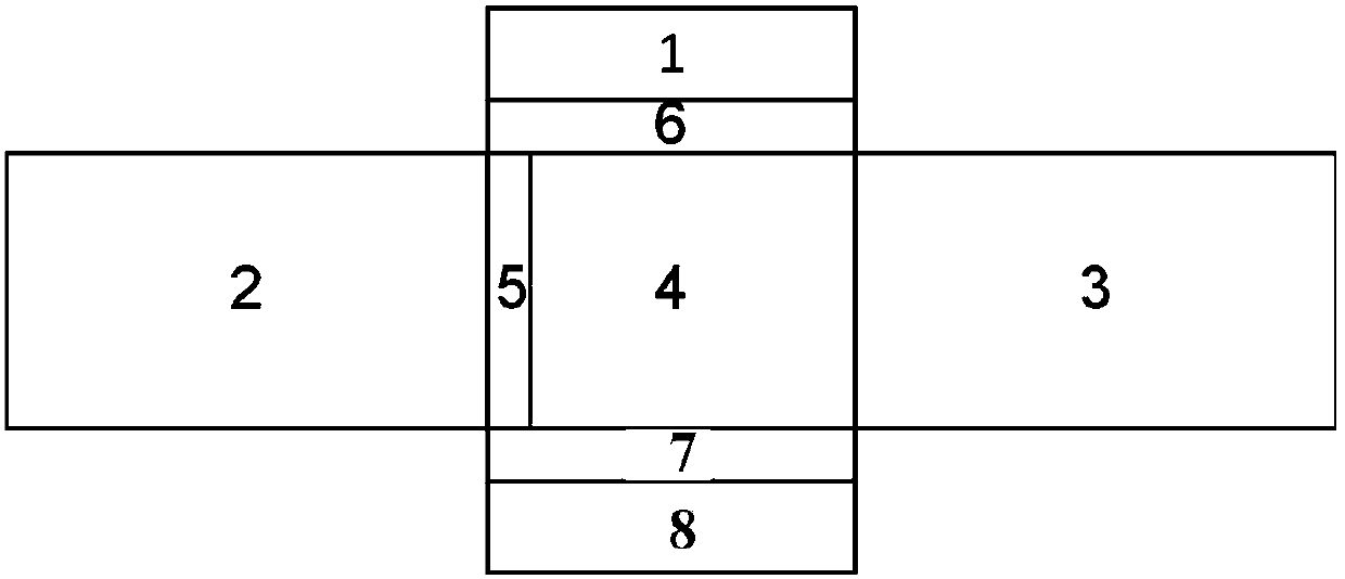
[0016] Such as figure 1 A Schottky junction tunneling field effect transistor is shown, comprising a first gate 1, a source region 2, a drain region 3, a channel region 4, a heavily doped pocket region 5, a first gate dielectric layer 6, a second A gate 8 and a second gate dielectric layer 7; wherein the upper and lower sides of the channel region 4 are respectively provided with a first gate dielectric layer 6 and a second gate dielectric layer 7; above the first gate dielectric layer 6 is provided with a first gate 1. A second gate 8 is provided under the second gate dielectric layer 7; the first gate 1, the first gate dielectric layer 6, the second gate 8 and the second gate dielectric layer 7 maintain vertical symmetry; the source region 2 and The drain region 3 is ...


PUM


Abstract

The invention discloses a schottky junction tunneling field effect transistor, which comprises a first gate, a source region, a drain region, a channel region, a heavily-doped pocket region, a first gate dielectric layer, a second gate and a second gate dielectric layer. Heavily-doped silicon or other semiconductor material is replaced with metal or metal silicide in the drain region to form a schottky contact on the contact surface of the drain region and a channel. Due to the presence of a schottky barrier, band bending of the channel region of a device becomes slow, and the width of a tunneling barrier of the device is increased. Due to the presence of the schottky barrier, electric field distribution in the channel region and the drain region of the device is effectively adjusted, and the electric field intensity near a schottky junction is reduced. Therefore, the short-channel effect can be effectively inhibited by the schottky junction tunneling transistor; and the schottky junction tunneling transistor still has a relatively good switching characteristic when the feature size is reduced to sub-10 nanometers.

Description

technical field [0001] The invention relates to a device for semiconductor integrated circuits, mainly a schottky junction tunneling field effect transistor. Background technique [0002] In order to make TFET devices can be used as ideal switching devices in ultra-low power consumption circuits, the reduction law of TFET device feature size must meet the International Technology Roadmap for Semiconductor (ITRS). However, with the continuous shrinking of the device feature size, the short-channel effect seriously affects the switching characteristics of the device. Since the region where band-band tunneling occurs in TFET devices is very small, traditional p-i-n structure TFET devices have good scalability even without the use of advanced technology. However, when the feature size of TFET is reduced to the range of sub-30 nanometers, the performance of the device will be seriously affected, which is mainly due to the formation of a certain intensity of electric field in the...

Claims


Application Information

Patent Timeline
Patent Type & Authority Patents(China)
IPC IPC(8): H01L29/10H01L29/423H01L29/739
CPCH01L29/1025H01L29/42312H01L29/7391
Inventor 王颖曹菲王艳福于成浩
Owner HANGZHOU DIANZI UNIV
Why Eureka
Try Eureka