A kind of preparation method of deep groove lateral withstand voltage region with longitudinal linear variable doping

A technology of lateral withstand voltage and withstand voltage region, which is applied in semiconductor/solid-state device manufacturing, semiconductor devices, electrical components, etc., and can solve problems such as difficult to achieve charge balance state and limit device performance

Active Publication Date: 2022-05-03
UNIV OF ELECTRONICS SCI & TECH OF CHINA
View PDF13 Cites 0 Cited by
  • Summary
  • Abstract
  • Description
  • Claims
  • Application Information

AI Technical Summary

Problems solved by technology

But the deep groove itself is capacitive, the semiconductor regions at both ends of the groove are the two plates of the capacitor, and the medium in the groove is the capacitor medium; since the potential difference on both sides of the deep groove gradually decreases from top to bottom, the deep groove capacitance caused by The charge concentration at the interface between the semiconductor and the deep groove also gradually decreases from top to bottom; at the same time, the types of charges at the interface between the semiconductor and the deep groove caused by the capacitance of the deep groove are opposite at the left and right ends of the groove; therefore, the deep groove The presence of capacitance makes such figure 1 It is often difficult to reach the charge balance state in the drift region of the deep trench lateral withstand voltage region shown, which limits the further improvement of device performance

Method used


Image

  • A kind of preparation method of deep groove lateral withstand voltage region with longitudinal linear variable doping
  • A kind of preparation method of deep groove lateral withstand voltage region with longitudinal linear variable doping
  • A kind of preparation method of deep groove lateral withstand voltage region with longitudinal linear variable doping

Examples


Embodiment 1

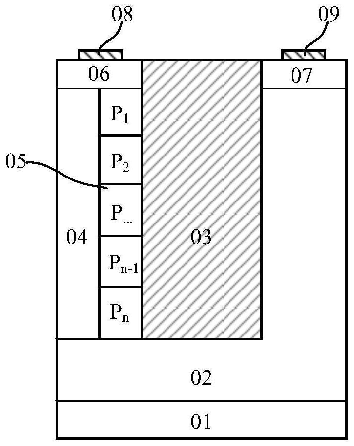
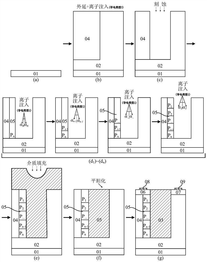
[0036] This embodiment provides a method for preparing a deep trench lateral voltage withstand region with longitudinal linearly variable doping on one side, and the structure of the deep trench lateral voltage withstand region with longitudinal linearly variable doping on one side is as follows Image 6 As shown, the specific process flow is as follows Figure 7 shown, including the following steps:

[0037] Step 1: Prepare before processing and clean the semiconductor;

[0038] Step 2: Perform epitaxy on the substrate 01 to form a withstand voltage region 04, such as Figure 7 as shown in (a);

[0039] Step 3: Etching the withstand voltage region 04 to form a first rectangular deep groove in the withstand voltage region, such as Figure 7 as shown in (b);

[0040] Step 4: Carry out epitaxy on the deep groove, and form a withstand voltage region 05 in the deep groove, such as Figure 7 as shown in (c);

[0041] Step 5: Process the chute on the pressure-resistant zone 05 t...

Embodiment 2

[0048] This embodiment provides a method for preparing a deep groove lateral voltage-sustaining region with longitudinal linear variable doping on both sides, the structure of the deep groove lateral voltage-sustaining region having longitudinal linear variable doping on both sides is as follows Figure 8 As shown, the specific process flow is as follows Figure 9 shown, including the following steps:

[0049] Step 1~step 9 are identical with embodiment 1;

[0050] Step 10: Carry out chute processing on the flat medium 03 and the pressure-resistant area 05 again to form a second chute in the shape of an "inverted trapezoid" with a narrow bottom and a wide top. The opening width of the second chute is w 3 , formed as Figure 9 (i) The chute shown in (i), the inclination angle of the chute is β, and the depth is h;

[0051] Step 11: Perform ion implantation with an inclination angle α on the side wall of the second chute processed in step 10, and form the following on the rig...


PUM


Abstract

The invention relates to the field of semiconductor power devices, and relates to a lateral pressure-resistant region, and specifically provides a method for preparing a deep groove lateral voltage-resistant region with longitudinally linearly variable doping, which is used to overcome the existing deep groove laterally with longitudinally linearly variable doping. The withstand voltage region can only realize the vertical variable doping in which the doping concentration changes stepwise with the vertical depth, which leads to the problem that its effect is not ideal. The deep trench lateral withstand voltage region prepared by the present invention has a vertical variable doping column region close to the ideal distribution, and by controlling the dose of ion implantation and the side wall inclination β, the electric field distribution of the withstand voltage region can be adjusted to make it close to the ideal superjunction The electric field distribution of the structure.

Description

technical field [0001] The present invention relates to the field of semiconductor power devices, relates to a lateral withstand voltage region, in particular to a longitudinal linear variable doping method for a deep trench lateral withstand voltage region; semiconductor power devices applicable to the lateral direction include LDMOS (Lateral Double-Diffused MOSFET), The process design of the withstand voltage region of LIGBT (Lateral Insulated Gate Bipolar Transistor). Background technique [0002] There is a deep groove filled with insulating medium in the deep groove lateral withstand voltage region. With this deep groove, the drift region can be folded, thereby increasing the effective length of the drift region and optimizing the device breakdown voltage and specific on-resistance. compromise relationship. [0003] In order to further optimize the deep trench lateral withstand voltage region, there is a deep trench lateral withstand voltage region structure with doped...

Claims


Application Information

Patent Timeline
Patent Type & Authority Patents(China)
IPC IPC(8): H01L21/265H01L29/06
CPCH01L29/0623H01L29/0634H01L29/0684H01L21/26586H01L21/265
Inventor 程骏骥武世英陈为真
Owner UNIV OF ELECTRONICS SCI & TECH OF CHINA
Why Eureka
Try Eureka