Die back surface silicone printing encapsulation method

A packaging method and wafer technology, applied in the direction of electrical components, semiconductor/solid-state device manufacturing, circuits, etc., can solve the problems of complex manufacturing process, expensive raw materials, and high prices, so as to reduce costs, improve bonding quality, and avoid The effect of glue layer voids

Inactive Publication Date: 2016-08-24
TEKISM
View PDF4 Cites 7 Cited by
  • Summary
  • Abstract
  • Description
  • Claims
  • Application Information

AI Technical Summary

Problems solved by technology

[0003] In order to solve the problems of complex manufacturing process, expensive raw materials and high prices in the prior art, the invention discloses a method of reducing material cost and overcoming the problems caused by dispensing. By brushing silica gel on the back of the wafer, it A packaging method of printing glue on the back of the wafer that is tightly combined with the substrate

Method used


Image

  • Die back surface silicone printing encapsulation method
  • Die back surface silicone printing encapsulation method
  • Die back surface silicone printing encapsulation method

Examples


Embodiment Construction

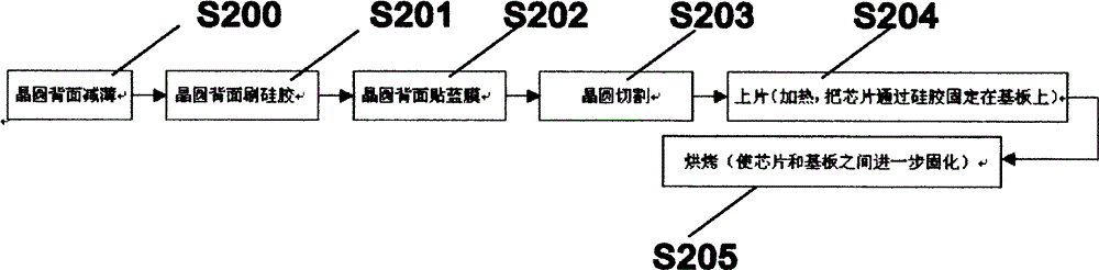
[0027] The present invention will be further described below in conjunction with the accompanying drawings. It should be understood that the specific embodiments described here are only used to explain the present invention, and are not intended to limit the present invention.

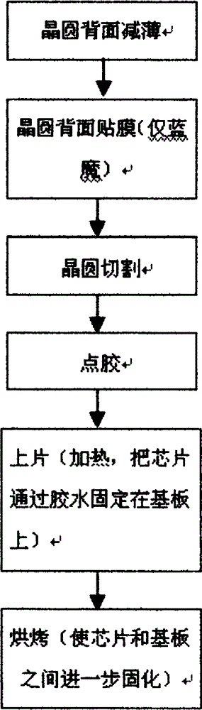
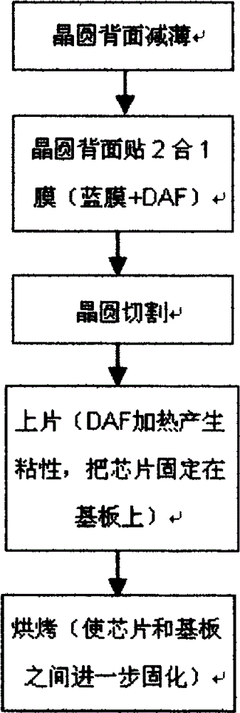
[0028] Such as figure 1 and figure 2 As shown, the existing method of wafer packaging in integrated circuits includes two conventional process methods, the first process: the wafer is pasted by DAF film, and the price remains high due to the complicated manufacturing process and expensive raw materials; and the second process In the second process, the wafer is pasted by the dispensing process. Because the dispensing process cannot ensure that the glue layer is uniform, it is easy to produce cavities. Especially for large chips, the probability of cavities is higher, and the cavities are larger, causing serious damage to subsequent processes. Interference poses a great risk to the stability of produc...


PUM


Abstract

The invention discloses a die back surface silicone printing encapsulation method, which adopts a die, a silicone layer and a substrate, and is used for carrying out thinning, silicone brushing, blue film adhering, cutting, die attaching and baking processes on the whole die. The die back surface silicone printing encapsulation method comprises the steps of thinning the back surface of the die, brushing the silicone on the back surface of the die, adhering the blue film on the back surface of the die, cutting the die, attaching the die and baking. The die back surface silicone printing encapsulation method is characterized in that: the die which is subjected to silicone brushing and blue film adhering on the back surface is cut into single die particles, the dependence of the die on the DAF film is changed, and direct material cost of die bonding is greatly reduced; and silicone layer cavities formed by uneven silicone dispersing process are avoided, reliability of the encapsulation technology is improved, and chip flatness after die bonding is increased, thereby being conductive to stabilizing a wire bonding process, reducing cost without increasing complexity of the processes, and improving bonding quality of the die and the substrate.

Description

technical field [0001] The invention relates to the technical field of integrated circuit packaging, and particularly discloses a packaging method for printing glue on the back of a wafer. Background technique [0002] At present, in the packaging of integrated circuits, conventional ICs, that is, integrated circuits, use semiconductor manufacturing technology to manufacture many transistors, resistors, capacitors and other components on a small single crystal silicon wafer, and follow the multi-layer wiring or tunnel A wiring method that combines components into a complete electronic circuit. Due to different processes, there are many ways to package integrated circuits. Among them, there are two types of pasting methods used in the die-bonding process in the packaging process: one process is to use the DAF film (DieAttach Film) on the back of the wafer, through the DAF film heat to bond the wafer to the substrate (eg figure 1 As shown), the wafer is fixed on the substrat...

Claims


Application Information

Patent Timeline
Patent Type & Authority Applications(China)
IPC IPC(8): H01L21/56
Inventor 凡会建李文化彭志文
Owner TEKISM
Why Eureka
Try Eureka