Method of quickly calculating far-field radiation field of large-scale MIMO array based on symmetric property
A fast computing, large-scale technology, applied in computing, design optimization/simulation, special data processing applications, etc., can solve the problems of difficult calculation and long time consumption of personal computer
- Summary
- Abstract
- Description
- Claims
- Application Information
AI Technical Summary
Problems solved by technology
Method used
Image
Examples
Embodiment 1
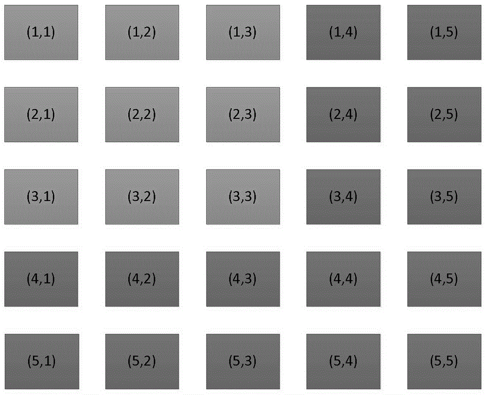
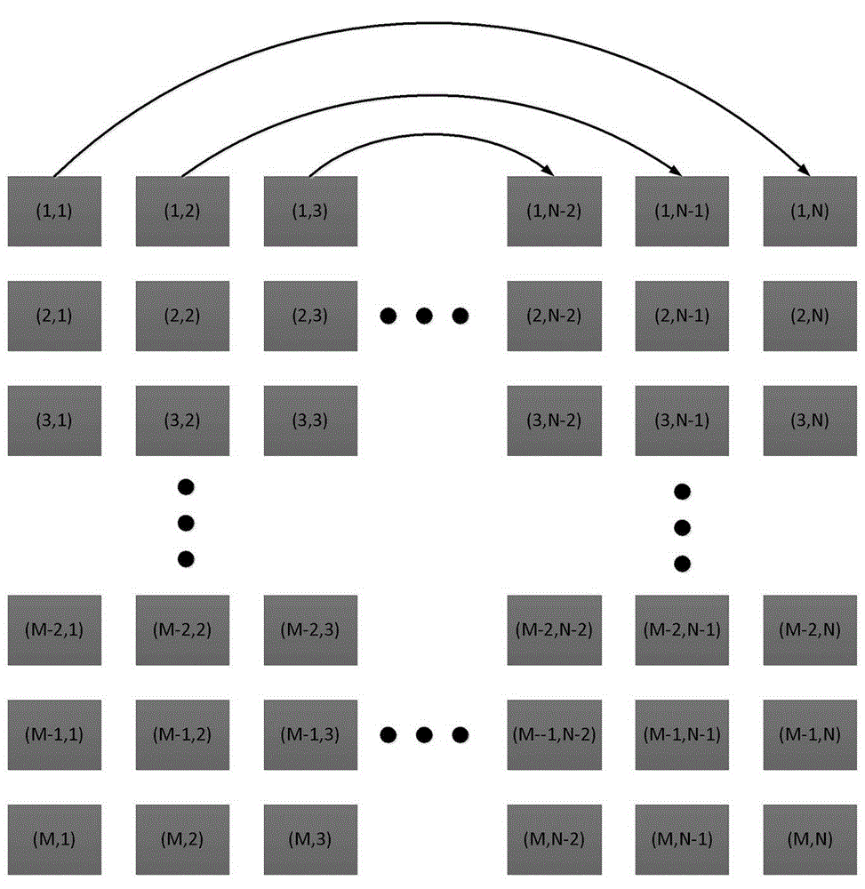
[0043] Example 1: Combining Figure 1-Figure 3 : A method for quickly calculating the far-field radiation field of a massive MIMO array based on symmetric characteristics, the method includes the following steps:
[0044] Step 1, determining the structure and parameters of the M×N element planar array antenna;
[0045] Determine the material, structure, operating frequency, spacing between planar array elements, and the number of rows and columns of a single antenna element.
[0046] Step 2, determining the sub-array size and extraction method in the large array;
[0047] For a large M×N array, a 5×5 array is used as a sub-array, where M is greater than 5 and N is greater than 5. For the calculation of the active unit pattern of each unit of the sub-array, the numerical algorithm or the HFSS software based on the finite element method are used for calculation; the full-wave simulation is carried out on the 5×5 small area array on the HFSS software, and only the ( 1, 1), (1,...
Embodiment 2
[0075] Example 2, combined with Figure 1-Figure 4 , Step 1. Determine the structure and parameters of the M×N element planar array antenna.
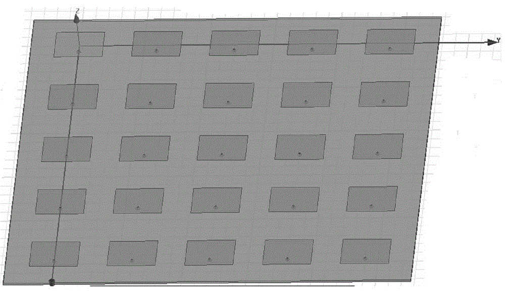
[0076] The coaxial feed patch antenna array is used to verify the correctness of the above method. The thickness of the dielectric substrate is 1.6mm, the length and width of the radiation patch are 28mm and 37.26mm respectively, the distance between the coaxial feed point and the center of the patch is 7mm, and the 1 / 4 working wavelength is 30mm. The HFSS design model of a rectangular microstrip antenna is as follows image 3 shown. The center of the model is located at the coordinate origin, the length direction of the radiation patch is along the x-axis direction, and the width direction is along the y-axis direction. The size of the dielectric substrate is twice that of the radiation patch. The reference ground and the radiation patch are replaced by ideal thin conductors. In HFSS, the ideal thin conductor is simulated by assigni...
PUM
 Abstract
Description
Claims
Application Information


