Antenna structure and design method thereof

An antenna structure and antenna array element technology, which is applied in the fields of electronics, radar, and microwave radio frequency, can solve the problems of system circuit board area increase, large radiation loss, cost increase, etc., to reduce production costs, eliminate switching time, The effect of reducing the size of the system

Active Publication Date: 2016-08-31
SOUTHEAST UNIV +1
View PDF3 Cites 15 Cited by
  • Summary
  • Abstract
  • Description
  • Claims
  • Application Information

AI Technical Summary

Problems solved by technology

[0009] The problem to be solved by the present invention is: to overcome the large-scale microstrip feed network used by the array antenna, which has relatively large radiation loss and mutual coupling in the millimeter wave frequency band, and proposes a The antenna structure overcomes the shortcomings of switching time, insertion loss, cost increase, and system circuit board area increase in the prior art when solving such problems, and gives the design method of the antenna structure

Method used


Image

  • Antenna structure and design method thereof
  • Antenna structure and design method thereof
  • Antenna structure and design method thereof

Examples


Embodiment Construction

[0032] Below in conjunction with accompanying drawing, the present invention is described in further detail:

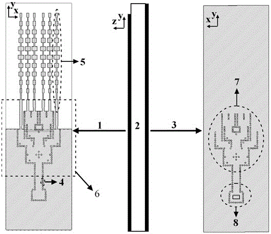
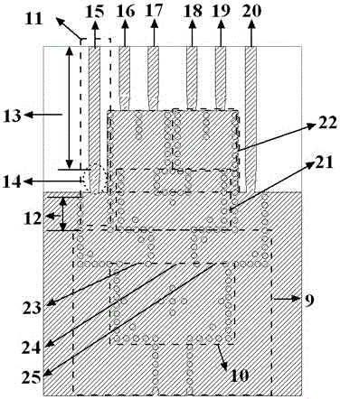
[0033] Such as figure 1 As shown, the hierarchical structure of the array antenna involved in the present invention includes an upper metal structure 1, a dielectric substrate 2 and a lower metal structure 3, wherein the metal layer is indicated by hatching. The functional structure of the entire array antenna includes a feeding network 6, a radiation unit 5 and a transition structure 8 from a substrate-integrated waveguide to a waveguide. There are six radiation units 5 forming an array along the x direction. Figure 4 shows metallized through-holes, in which the radiation unit 5 adopts the structural form of a serially fed microstrip array, and the feed network 6 includes a substrate-integrated waveguide power divider 7 and a phase shifter 11, and the substrate The integrated waveguide-to-waveguide transition structure can connect the entire array antenna structure ...


PUM


Abstract

The invention discloses an antenna structure and a design method thereof, wherein the antenna structure comprises a radiation unit and a feed network. An output end of the feed network is connected with an input end of the radiation unit. The feed network is of an axisymmetric structure. The feed network comprises one-to-multiple substrate integrated waveguide power divider and a phase shifter. The phase shifter is connected to multiple output ends of the substrate integrated waveguide power divider. The radiation unit is of a symmetric structure with the symmetric axis of the feed network serving as the center and is connected to the tail end of the phase shifter. The antenna structure overcomes the problems of a relatively large-scale microstrip feed network that the relatively large radiation loss and cross coupling exists in the millimeter wave frequency band, the antenna can also meet middle distance and long distance test requirements of a radar, switching time existing in other schemes is eliminated, the cost is low, and the size is small.

Description

[0001] The invention relates to the fields of electronics, microwave radio frequency, radar and the like, and in particular relates to a structure and a design method of a novel array antenna. Background technique [0002] current technology [0003] Array antennas are used in many occasions due to their advantages of high gain and beamforming, such as radar, communication, navigation, etc. The design of the feed network is a very important part of the design of the array antenna. Microstrip transmission lines are used as a This traditional transmission line form has been widely used, especially in the feed network design of some array antennas. In some special applications, an array form with a large number of array elements and a relatively complex feed network are required. For the millimeter-wave frequency band with high frequency, the complex feed network will not only greatly increase the difficulty of design, but also greatly The large-scale use of microstrip feeding w...

Claims


Application Information

Patent Timeline
Patent Type & Authority Applications(China)
IPC IPC(8): H01Q23/00H01Q1/38H01Q1/50H01Q21/00
CPCH01Q1/38H01Q1/50H01Q21/00H01Q21/0087H01Q23/00
Inventor 洪伟徐俊张慧
Owner SOUTHEAST UNIV
Why Eureka
Try Eureka