Plasma treatment device and wafer transportation tray

A processing device and plasma technology, which is applied in the direction of plasma, semiconductor/solid-state device manufacturing, discharge tube, etc., can solve problems such as troublesome operation, reduced adhesion between the tray for wafer transfer and the support body, etc., to reduce loss and reduce mechanical The effect of permanent movable parts and efficient cooling

Active Publication Date: 2016-08-31
ULVAC INC
View PDF5 Cites 3 Cited by
  • Summary
  • Abstract
  • Description
  • Claims
  • Application Information

AI Technical Summary

Problems solved by technology

Therefore, there is a problem that the operation when fixing the wafer transfer tray to the support body is troublesome.
In particular, in terms of structure, since the mechanical jig is fixed in contact with the peripheral portion of the wafer transfer tray, the adhesion between the wafer transfer tray and the support body decreases near the center of the wafer transfer tray.

Method used


Image

  • Plasma treatment device and wafer transportation tray
  • Plasma treatment device and wafer transportation tray
  • Plasma treatment device and wafer transportation tray

Examples


no. 1 approach

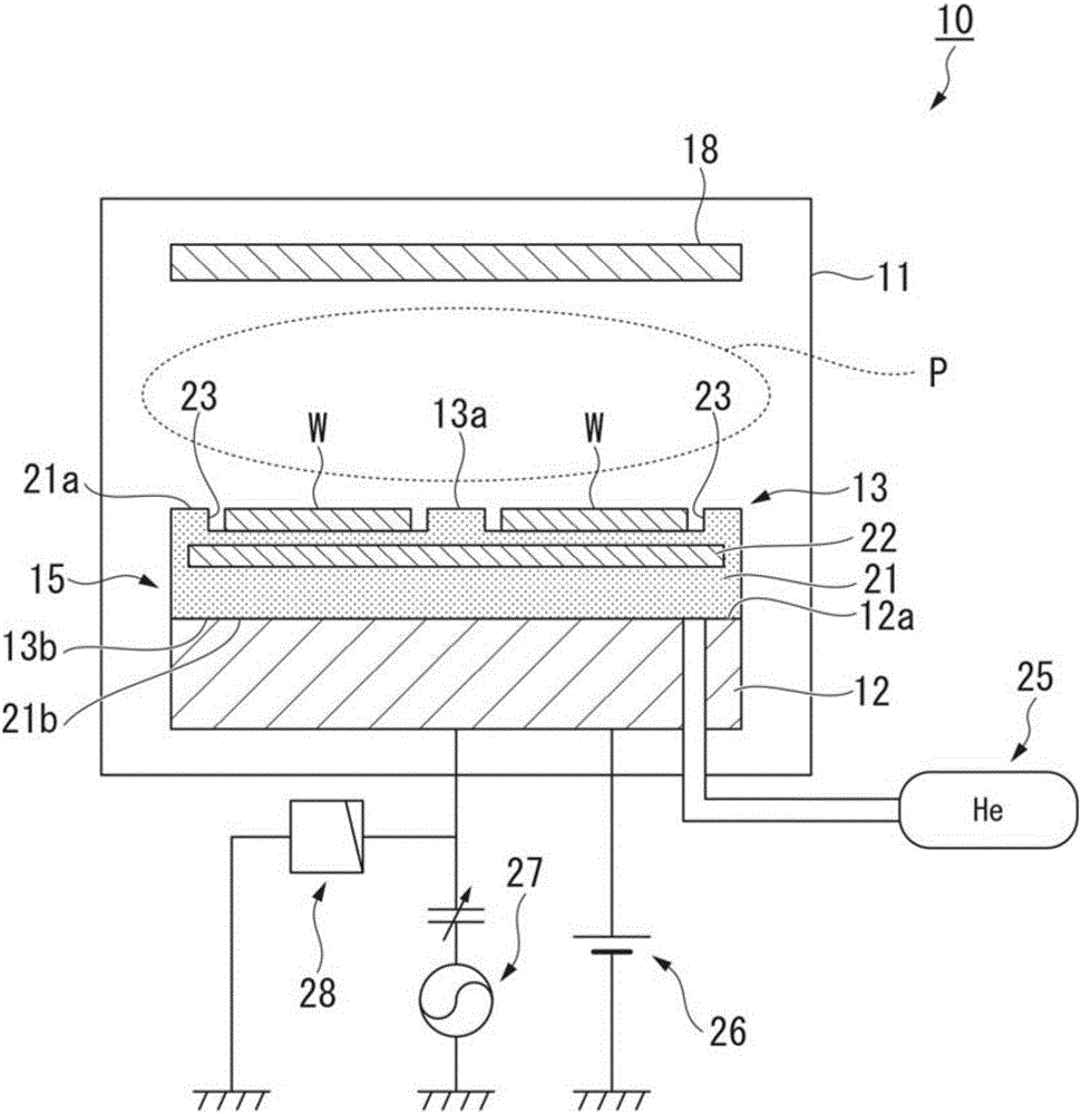
[0035] figure 1 It is a sectional view showing the whole plasma processing apparatus according to the first embodiment of the present invention.

[0036]The plasma processing apparatus 10 includes: a plasma processing tank (chamber) 11; an upper electrode 18 disposed near the upper surface inside the plasma processing tank 11; a support body 12 disposed near the bottom surface inside the plasma processing tank 11, And the lower electrode is formed; and the supporting part 15 has the tray 13 for wafer transfer placed on the supporting body 12 .

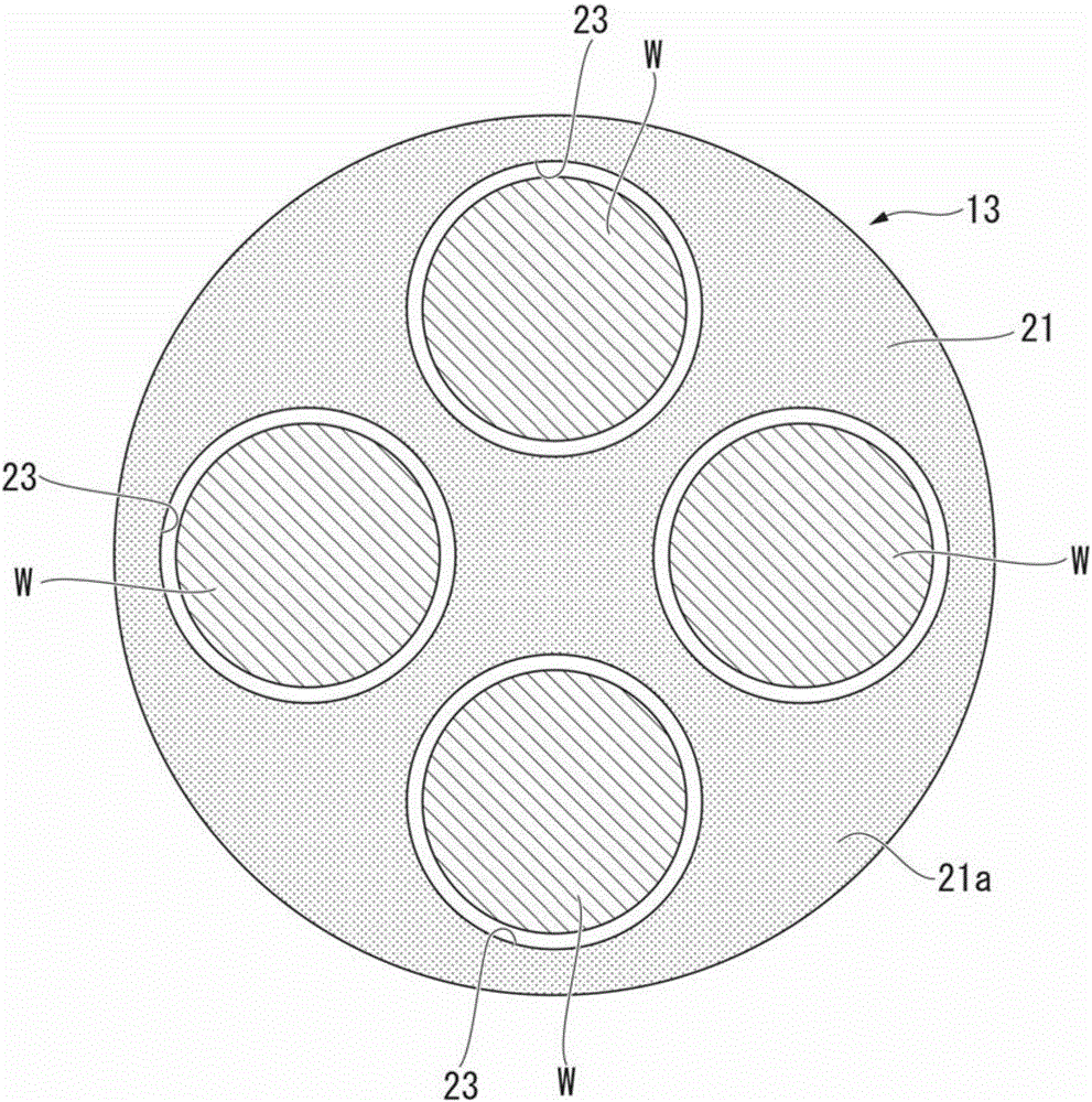
[0037] The tray 13 for wafer transfer has: a substantially disk-shaped base 21; ) The position of 21a. Further, on one surface 21a of the base body 21, a concave portion 23 for inserting a wafer W which is an object to be processed is formed.

[0038] Substrate 21 has a resistance value of 10 8 More than Ω and 10 11 It is composed of a high resistance body in the range of Ω or less.

[0039] Such a high resistance body may be, fo...

no. 2 approach

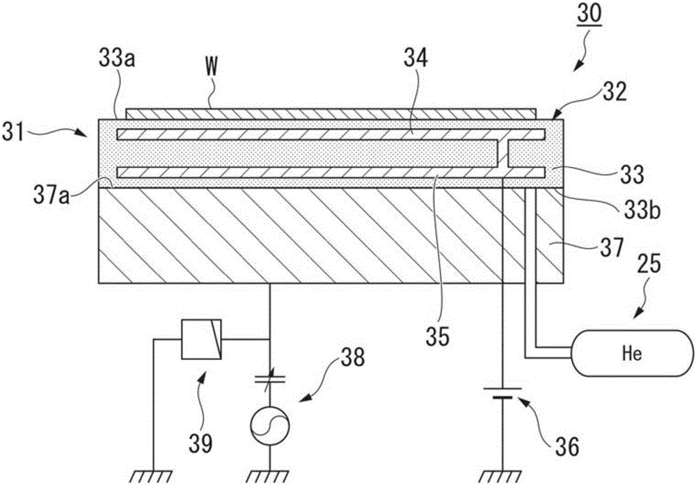
[0063] image 3 It is a cross-sectional view showing the vicinity of the support portion of the plasma processing apparatus according to the second embodiment of the present invention.

[0064] The wafer transfer tray 32 in the support portion 31 of the plasma processing apparatus 30 according to the second embodiment includes: a base 33 formed of an insulator; The other surface 33b is closer to the position of one surface (first surface) 33a; and the second conductive layer 35 for electrostatic adsorption is embedded in the position of the substrate 33 closer to the other surface (second surface) 33b than the one surface 33a. .

[0065] The base body 33 is made of, for example, a ceramic plate or the like. The first conductive layer 34 and the second conductive layer 35 are electrically connected by a conductor extending in the thickness direction of the wafer transfer tray 32 .

[0066] The first conductive layer 34 and the second conductive layer 35 are made of metals su...

no. 3 approach

[0083] Figure 4 It is a sectional view showing the vicinity of the support portion of the plasma processing apparatus according to the third embodiment of the present invention.

[0084] The tray 42 for wafer transfer in the support portion 41 of the plasma processing apparatus 40 according to the third embodiment has: a base 43 formed of an insulator; The other surface 43b is closer to the one surface (first surface) 43a; and the conductor 45 is disposed so as to be exposed on the other surface (second surface) 43b of the base body 43 .

[0085] The base body 43 is made of, for example, a ceramic plate or the like. The first conductive layer 44 and the conductor 45 are made of metals such as aluminum, tungsten, titanium, or alloys containing these metals. The first conductive layer 44 may be formed, for example, at a position several millimeters deep from the one surface 43 a of the base 43 so as to extend parallel to the one surface 43 a of the base 43 .

[0086] Such a ...


PUM


Abstract

This plasma treatment device is provided with: a wafer transportation tray having a first surface and a second surface opposite the first surface, the wafer transportation tray holding the wafer on the first surface; a cooling unit for cooling the wafer transportation tray; an electroconductive support body for supporting the second surface of the wafer transportation tray; and a double-sided electrostatic suction unit for electrostatically chucking the wafer on the first surface of the wafer transportation tray and electrostatically chucking the support body on the second surface of the wafer transportation tray.

Description

technical field [0001] The present invention relates to a plasma processing apparatus and a wafer transfer tray, and more specifically, to fixing of a wafer transfer tray. [0002] This application claims priority based on Japanese Patent Application No. 2014-009682 for which it applied in Japan on January 22, 2014, and uses the content here. Background technique [0003] Conventionally, in the manufacture of semiconductor devices, when a plurality of wafers etc. were collectively processed by plasma processing, it was usually performed using a wafer transfer tray. For example, a plurality of wafers are placed on one surface of the wafer transfer tray. Such a wafer transfer tray is placed on a support body of a plasma processing apparatus. The support functions as one electrode during plasma treatment. [0004] When plasma processing is performed on a wafer by a plasma processing apparatus, if a pressing unit is used to fix the wafer to the wafer transfer tray, not only t...

Claims


Application Information

Patent Timeline
Patent Type & Authority Applications(China)
IPC IPC(8): H01L21/673H01L21/3065H01L21/683
CPCH01L21/6831H01L21/68771H01L21/67103H01L21/67109H01L21/6833H01J37/32724H01J37/32733H01L21/02315H01L21/6773H05H1/46H01L21/67069H01L21/67098H01L21/67313H01L21/67333
Inventor 中村敏幸森口尚树上村隆一郎长田大和相原强
Owner ULVAC INC
Why Eureka
Try Eureka